标签:des style blog http color os strong io
Described herein is a method and an apparatus for training a memory signal via an error signal of a memory. The method comprises transmitting from a memory controller a command-address (C/A) signal to a memory module; determining by the memory controller an error in the memory module via an error signal from an error pin of the memory module, the error associated with the C/A signal transmitted to the memory module; and modifying by the memory controller the C/A signal in response to determining an error in the memory module, wherein the error pin is a parity error pin of the memory module, and wherein the memory module comprises a Double Data Rate 4 (DDR4) interface.
Embodiments of the invention relate generally to the field of memory controllers. More particularly, embodiments of the invention relate to a method and an apparatus for training a command-address (C/A) memory signal via a C/A parity error signal from a memory.
In a typical memory system of a computer system, a memory controller facilitates the access of a memory module in the computer system. The memory module may include one or more memories. These one or more memories are also called ranks. The memory controller transmits a host of signals to the ranks including address signals, control signals, clock signals, etc., to access data from the ranks or to send data to the ranks. To send and receive correct data to and from the ranks, the memory controller trains (modifies) the command-address (C/A) signals with respect to a clock signal.
Typically, the memory controller trains the C/A signals by transmitting a particular C/A signal with respect to a clock signal to the ranks and then analyzing a response from each rank to ascertain if the rank correctly received the particular C/A signal. Upon a successful/correct response from the rank, the memory controller delays the phase of the particular C/A signal with respect to the clock signal and then re-transmits the delayed particular C/A signal with a delayed phase to the rank. The memory controller then analyzes a response from the rank to ascertain if the rank correctly received the delayed particular C/A signal. If no response (or an incorrect response) is received from the rank to the memory controller, the memory module transitions to an unknown state (indeterminate state) resulting in a non-functional memory module.
In case of a Double Data Rate 3 (DDR3) memory interface between the memory controller and the memory module having the ranks, the unknown state of the memory module is resolved to a known state by a Joint Electron Devices Engineering Council (JEDEC) standardized initialization process. The JEDEC standardized initialization process results in resetting the memories.
The JEDEC standardized initialization process is a time consuming process that takes several milliseconds for the memory controller to restore the memory module to a known functional state. As computing requirements by users are becoming more memory usage intensive, any error in the memory system e.g., error caused by a C/A signal (with a phase with respect to a clock signal that results in accessing incorrect data from the memory module to the memory controller) results in loss of time due to the time consuming JEDEC standardized initialization process which is required for the DDR3 based memory interface. Furthermore, as demand for faster boot-up of memory systems is increasing, such errors may lead to intolerable lengthening of boot-up time as experienced in a DDR3 based memory interface.
Embodiments of the invention relate to a method and an apparatus for training a memory signal via an error signal of a memory.
In one embodiment, the memory is part of a memory module having one or more memories. In one embodiment the memory signal is a command-address (C/A) signal and the corresponding error signal is a parity error signal. In one embodiment, the voltage level of the parity error signal indicates if there is an error in the memory module requiring the C/A signal to be re-trained to resolve the error without initiating a JEDEC standardized initialization process. In one embodiment of the invention, the memory module includes a Synchronous Dynamic Random Access Memory (SDRAM), Dynamic Random Access Memory (DRAM), RAMBUS Dynamic Random Access Memory (RDRAM), double-data-rate four SDRAM (DDR4), and any other type of random access memory device.
So as not to obscure the embodiments of the invention, the embodiments herein are discussed with reference to a Dual In-Line Memory Module (DIMM) having one or more SDRAMs, which are also called ranks, where the DIMM is communicatively coupled to the memory controller via a DDR4 I/O interface. In one embodiment, the DIMM comprises SDRAM(s) arranged as one, two, or four ranks. In other embodiments, other arrangements of SDRAM ranks may be used. However, the above embodiments are not limiting embodiments. Other embodiments having different memory modules (other than the DIMM), ranks without memory modules, and other I/O interfaces (newer than the DDR4 I/O interface) can be used without changing the essence of the invention.
FIG. 1?is a memory system?100?comprising a memory controller?101?operable to train a C/A signal?104?via an error signal?105, and a memory module?102coupled to the memory controller, according to one embodiment of the invention. In one embodiment, the memory controller?101?is integrated within a microprocessor (CPU). In other embodiments, the memory controller?101?is a separate integrated circuit (IC) on the motherboard and is coupled to the CPU (not shown) and the memory module?102. In one embodiment of the invention, the memory module?102?includes DRAMs (111?1-N), register devices, buffer devices, etc. In one embodiment, the memory controller?101?communicates with the memory module?102?via signals including, but not limited to, C/A signal?104, C/A parity error signal?105, control signals?107, data signals?108, clock signals109, parity signal?110, and any other signals to cause communication between the memory controller?101?and the memory module?102.
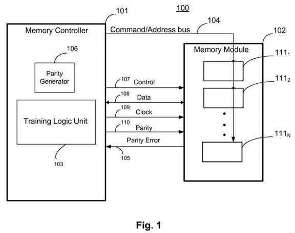
In one embodiment of the invention, when the memory controller?101?transmits a command signal (e.g., read, write, etc.,) to the memory module?102, the memory controller?101?computes a parity of address signal bits and command signal bits of the command signal via a parity generator?106. In one embodiment, the parity generator?106?determines a parity bit signal?110?based on an even or odd parity of a combination of the computed parity and the parity bit signal. In one embodiment, the parity generator?106?provides the parity for the signals including but not limited to, row address strobe (RAS) signal, column address strobe (CAS) signal, write enable (WE) signal, address bus signals, and bank select signals of the memory module?102.
In one embodiment, the memory controller?101?provides the parity bit signal as one of the parity signals?110?when a command is sent/transmitted to the memory module?102?from the memory controller?101. In one embodiment, the memory module?102, upon receiving a command signal and its corresponding parity signal, is operable to detect or determine if the received command signal has any C/A parity error. The term command signal and command are herein used interchangeably.
In one embodiment, when the memory module?102?detects a parity error in the received command signal, it ignores the received command signal and stores the command bits and the address bits of the received command signal in a mode register. In one embodiment, the memory module?102?asserts an error signal?105?to the memory controller?101?when the parity error in the received command signal is detected.
In one embodiment, the error signal?105?is a parity error signal which is feedback from the memory module?102?to the memory controller?101. In one embodiment, the parity error signal?105?is an ALERT# signal of the DDR4 I/O interface between the memory controller?101?and the memory module?102.
In one embodiment, the memory controller?101?comprises a training logic unit?103?operable to receive the parity error signal105?from the memory module?102?and to determine from the parity error signal?105?whether a parity error is present in the received command. In one embodiment, the parity error signal?105?is a C/A parity error signal. In one embodiment, an error handling mechanism is triggered to recover from the errant command (because of the parity error) and the training logic unit103?begins to train the C/A signal?104?without initiating a reboot of the memory system?100?or a JEDEC standardized initialization process.
So as not to obscure the embodiments of the invention, the embodiments herein refer to the parity error signal?105?as the C/A parity error signal?105?to indicate that the parity error is a C/A parity error.
With C/A parity support in the memory module?102, the performance of the memory system?100?is improved because the memory system?100?does not need to be rebooted nor does a JEDEC standardized initialization process need to be initiated in order to recover the memory system?100?from an errant command received by the memory module?102?and to retrain the C/A signal?104. The training process of the C/A signal?104?via the embodiments herein is much faster than a memory system having no support for the C/A parity error signal?105.
For example, the training of the C/A signal?104?is completed via the embodiments herein within a few nanoseconds (e.g., about 200 nanoseconds) compared to milliseconds or more to train the C/A signals with a memory module having no support for C/A parity i.e., an order magnitude of difference in speed of training the C/A signal with the embodiments discussed herein. The faster training of the C/A signal?104?is because the reset sequence is avoided which may take up to a few seconds if initiated via software e.g., Basic Input-Output System (BIOS).
While the memory system?100?is illustrated as a fly-by memory topology with a serial C/A signal?104, other topologies may be used without changing the essence of the embodiments of the invention.
FIG. 2?illustrates a logic level diagram?200?of the memory controller?101?operable to train the C/A signal?104?via the C/A parity error signal?105, according to one embodiment of the invention. The memory controller?101?comprises the training logic unit?103?which is operable to train the C/A signal?104?with respect to a clock signal?109. In one embodiment, the clock signal?109?is generated by a clock generator?206. In one embodiment, the training logic unit?103?comprises an Error Detection Logic?201?which is operable to detect a C/A parity error signal?105?from the memory module?102?of?FIG. 1.
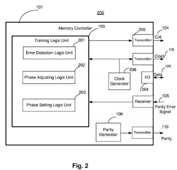
In one embodiment, the memory controller?101?further comprises I/O transceivers?204?which are operable to transmit and receive data signals?108?to and from the memory module?102. In one embodiment, the I/O transceivers?204?are DDR4 based I/O transceivers. In one embodiment, the C/A signal?104?is transmitted by the memory controller?101?to the ranks?1111-N?of the memory module?102?via a DDR4 based I/O interface. In one embodiment, the parity error signal?105?is received by the memory controller?101?from the memory module?102?via a receiver.
In one embodiment, the training logic unit?103?also comprises a phase adjusting logic unit?202?which is operable to adjust a phase of the C/A signal?104?with respect to the clock signal?109. In another embodiment, the phase adjusting logic unit?202is operable to adjust the phase of the clock signal?109?relative to a phase of the C/A signal?104. In one embodiment, the phase of the C/A signal?104?and/or the clock signal?109?is adjusted by delaying the C/A signal?104?and/or the clock signal109?with respect to one another via a delay unit (not shown). In one embodiment, the delay unit comprises a delay locked loop (DLL) with phase interpolators (PI) to adjust the phase of the C/A signal?104?and/or the clock signal?109?with respect to one another.
The term delay herein refers to positive and negative delay in time domain, where positive delay refers to adding a delay in time domain to a signal with respect to another signal while negative delay refers to pulling in a signal in time domain with respect to another signal. So as not to obscure the essence of the embodiments, details of how the phases of either the C/A signal?104?or the clock signal?109?are adjusted (delayed positively and/or negatively) with respect to one another is not discussed herein.
In one embodiment, the phase adjusting logic unit?202?is operable to adjust the C/A signal?104?by delaying (positively and/or negatively) a phase of the C/A signal?104?with respect to the clock signal?109?to generate an adjusted C/A signal. In one embodiment, the adjusted C/A signal (also referred to as the signal?104) is transmitted via a transmitter to the memory module?102. In one embodiment, in response to the transmitted adjusted C/A signal?104, the C/A parity signal?105?is monitored by the error detection logic unit?201. If no error is detected by the error detection logic unit?201, the phase adjusting logic unit?202?further delays a phase of the adjusted C/A signal?104?to generate another adjusted C/A signal (also referred to as?104) which is then transmitted to the ranks?111?1-N?of the memory module?102. In the above embodiment, the process of delaying (positively and/or negatively) the phase of the C/A signal?104?with respect to the clock signal?109?is repeated till the error detection logic unit?201?detects an error in the C/A parity signal?105. At that point, the training logic unit?103?determines a phase setting of the C/A signal?104?and the training of the C/A signal?104?completes.
In one embodiment, the training logic unit?103?further comprises a phase setting logic unit?203?which is operable to compute an average of phases of all correctly received C/A signals transmitted via transmitters?205?to the memory module?102, where the average of phases is used to compute a phase setting for C/A signals?104.
FIG. 3?illustrates the process?300?of training the C/A signal?104?with respect to the clock signal?109, according to one embodiment of the invention. The process?300?is illustrated with reference to embodiments of?FIG. 1?and?FIG. 2. The process?300?is divided into three scenarios:?301,?302, and?303. To reduce redundancy in describing the three scenarios, the process?300?shows positively delaying the C/A signal?304?relative to the clock signal?109. The C/A signal?304?is also delayed negatively (i.e., pulled-in) in time domain (not shown) with respect to the clock signal?109?during the training process.
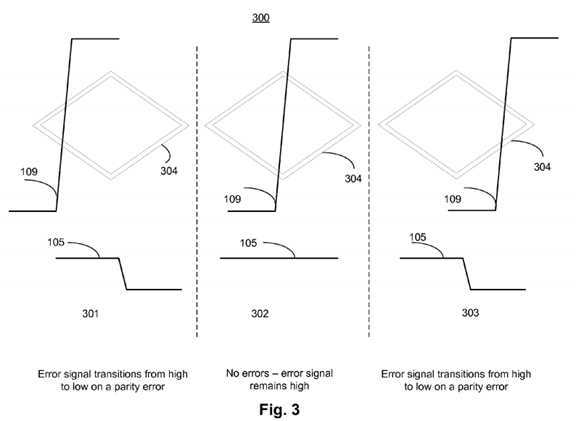
In the first scenario?301, the C/A signal?304?(which is the same as signal?104?but illustrated as an eye diagram) is located to the left of the clock signal?109?by the phase adjusting logic unit?202?of?FIG. 2. In this scenario, the C/A parity error signal105?transitions from a logical high level to a logical low level to indicate that there is a C/A parity error. In one embodiment, the phase setting logic unit?203?keeps track of the delay setting to the C/A signal?304?that resulted in an error indicated by the C/A parity error signal?105.
In the second scenario?302, the C/A signal?304?is adjusted by the phase adjusting logic unit?202?so that the transition point of the clock signal?109?is located in the middle of the eye of the C/A signal?304. In this scenario, the C/A parity error signal105?remains constant which indicates no error in the C/A parity. In one embodiment, the phase setting logic unit?203?keeps track of the delay setting to the C/A signal?304?that resulted in no error indicated by the C/A parity error signal?105.
In the third scenario?303, the C/A signal?304?is adjusted by the phase adjusting logic unit?202?so that the transition point of the clock signal?109?is located to the right of the eye of the C/A signal?304. In this scenario, the C/A parity error signal?105transitions from a logical high level to a logical low level which indicates an error in the C/A parity. In one embodiment, the phase setting logic unit?203?keeps track of the delay setting to the C/A signal?304?that resulted in an error indicated by the C/A parity error signal?105.
While the above process?300?is illustrated with the C/A parity error signal?105?transitioning from a logical high level to a logical low level to indicate a C/A parity error, alternative embodiments may indicate a C/A parity error when the C/A parity error signal?105?transitions from a logical low level to a logical high level without changing the essence of the embodiments of the invention.
Referring back to?FIG. 2, in one embodiment, the phase setting logic unit?203?is operable to compute an average of phases of all correctly received C/A signals transmitted to the memory module?102, where the average of phases is used to compute a new phase setting for C/A signals?104?resulting in training the C/A signal?104?with respect to the clock signal?109. In another embodiment, the phase setting logic unit?203?is operable to compute a phase setting that provides the most timing margin for the C/A signal?104?relative to the clock signal?109. In one embodiment, the phase setting logic unit?203?is operable to compute a phase setting that provides the most voltage margin for input receivers of the memories receiving the C/A signal?104?by adjusting (raising or lowering) the Voltage Reference (Vref) level of the input receivers receiving the C/A signal?104.
In other embodiments, different criteria can be used to assign a phase setting to the C/A signal?104?with respect to the clock signal?109?in view of the phases of the C/A signal?104?that result in no C/A parity error. In one embodiment, once a phase setting is computed by the phase setting logic unit?203, the phase setting is assigned to the C/A signal?104?for all memories (also referred to as ranks) of the memory module.
FIG. 4?is a high level method flowchart?400?for training the C/A signal?104?in response to the error signal?105, according to one embodiment of the invention. The flowchart is discussed with respect to the embodiments of?FIGS. 1-2.
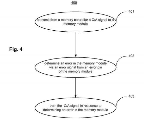
At block?401, the memory controller?101?transmits the C/A signal?104?to the memory module?102. A person skilled in the art would appreciate that the same C/A signal?104?is received by all memories (also referred to as ranks) in the memory module102. At block?402, the memory controller?101?determines via the error detection logic unit?201?an error in the memory module?102?from an error signal (parity error signal?105) via an error pin of the memory module?102, wherein the error is associated with the C/A signal?104?transmitted to the memory module?102. As mentioned above, in one embodiment the error pin corresponds to a parity error pin. In one embodiment, the error pin is an ALERT# pin of a DDR4 I/O interface. At block?403, the memory controller?101?trains the C/A signal?104?in response to determining an error in the memory module102.
FIG. 5A?is a detailed method flowchart?500?for training (modifying) the C/A signal?104?in response to the error signal?105, according to one embodiment of the invention. The flowchart is discussed with respect to the embodiments of?FIGS. 1-3.
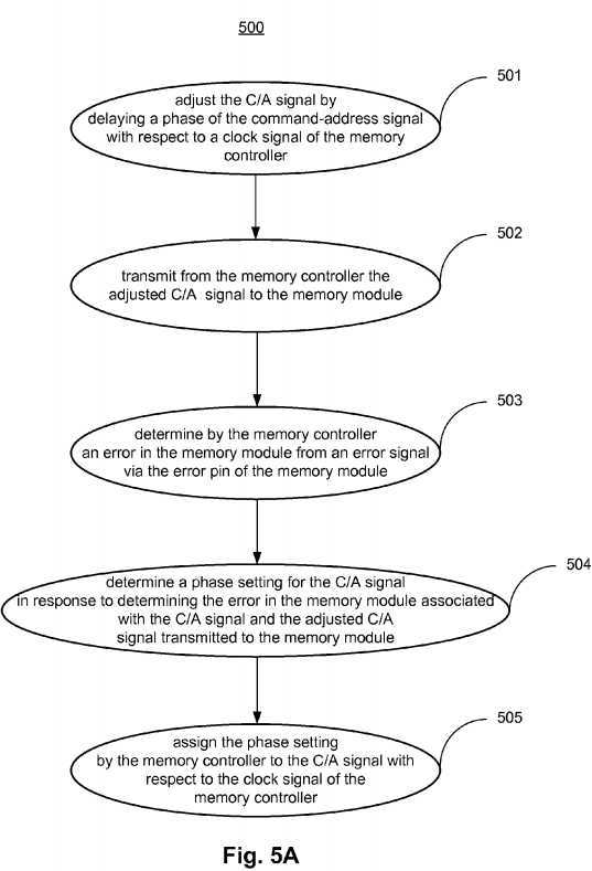
At block?501, the memory controller?101?trains the C/A signal?104?by adjusting the C/A signal?104. As discussed above, the C/A signal?104?is adjusted by a phase adjusting logic unit?202?which is operable to delay a phase of the C/A signal with respect to the clock signal?109. At block?502, the memory controller?101?transmits the adjusted C/A signal?104?to the memory module?102. At block?503, the memory controller?101?determines an error in the memory module?102?from an error signal via an error pin of the memory module?102, where the error is associated with the adjusted C/A signal transmitted to the memory module?102.
At block?504, the phase setting logic unit?203?determines a phase setting for the C/A signal in response to determining the error in the memory module?102?(which is discussed with reference to?FIG. 2?and?FIG. 3). In one embodiment, the phase setting indicates a setting of the phase interpolators (discussed with reference to?FIG. 2). Referring back to?FIG. 5A, at block?505, the phase setting logic unit?203?computes an average of the phases of all correctly received C/A signals?104transmitted by the memory controller?101?to the memory module?102.
In one embodiment, a control signal is trained prior to training the C/A signal?104?to isolate the errors detected during the training of the C/A signal?104—the errors are not caused by the control signal because it is trained prior to training of the C/A signal?104. In one embodiment, the control signal is a chip-select signal.
In one embodiment, the method of training the control signal comprises positioning a clock signal transition edge at a time point midway through a phase of the control signal. In one embodiment, in response to the positioning of the clock signal transition edge, the method of training the control signal further comprises issuing by the memory controller?101?the control signal to the memory module in response to the positioning. In one embodiment, in response to issuing the control signal by the memory controller, the memory controller?101?adjusts the phase of the control signal relative to the clock signal transition edge so long as the control signal is correctly received by the memory module.
In one embodiment, in response to adjusting the phase of the control signal, the memory controller?101?determines the phase of the control signal resulting in an incorrectly received control signal by the memory module. In one embodiment, in response to determining the phase of the control signal, the memory controller?101?positions the phase of the control signal relative to the clock signal transition edge. In such an embodiment, the positioning of the phase of the control signal relative to the clock signal transition edge comprises positioning the phase of the control signal based on an average of all adjusted phases of the control signal correctly received by the memory module.
While the methods of?FIG. 4?and?FIG. 5A?are discussed for a single memory unit (rank) in the memory module?102, the methods are repeated for each rank (111?1-N?of?FIG. 1) in the memory module?102?as shown by?FIG. 5B?to achieve a common trained phase setting for the C/A signal which is applied to all ranks (111?1-N?of?FIG. 1) in the memory module?102.
FIG. 5B?illustrates a method flow chart?510?for training the C/A signal?104?for a memory module having multiple ranks (e.g.,111?1-N?of?FIG. 1), according to one embodiment of the invention. The flowchart is discussed with respect to the embodiments of?FIGS. 1-2.
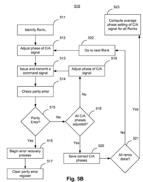
At block?511, the memory controller?101?identifies the first rank?111?1?of the memory module?102?for C/A training purposes. As mentioned above, C/A training process comprises adjusting by a phase adjusting logic unit?202?the phase of the C/A signal?104?with respect to a clock signal?109. At block?512, the phase adjusting logic unit?202?sets or adjusts the phase of the C/A signal?104?with respect to a clock signal?109?for the first selected rank?111?1?of the memory module?102. At block?513, the adjusted C/A signal (e.g., a read command signal with its corresponding address) is transmitted by a transmitter to the first rank?111?1?of the memory module?102.
At blocks?514?and?515, the error detection logic unit?201?determines if the parity error signal?105?indicates a parity error caused by the adjusted phase of the C/A signal?104. If a parity error is detected by the error detection logic unit?201, then at block?516?an error recovery process begins. As part of the error recovery process, at block?517, a parity error register within the memory controller is cleared or reset by a reset logic unit (not shown) of the memory controller?101?and the process moves block?518. At block?518, the memory controller determines if all phases of the C/A signal?104?have been adjusted by the phase adjusting logic unit?202.
If all the phases of the C/A signal?104?have been adjusted and parity error for each adjusted phase has been determined by the memory controller?101, then at block?520?all valid or correct C/A phases are saved in memory or a register for the selected ranks?111?1?of the memory module?102. As mentioned above with reference to?FIG. 3, valid or correct C/A phases refer to the C/A phases that resulted in a logical high state of the parity error signal?105.
If all phases of the C/A signal have not been adjusted by the phase adjusting logic unit?202, then at block?519?the phase adjusting logic unit?202?adjusts the phase of the C/A signal?104?by delaying the phase of the C/A signal?104?relative to the clock signal?109. The process control then transfers to block?513?at which the C/A signal?104?(e.g., a read command signal with its corresponding address) is transmitted by a transmitter to the first rank?111?1?of the memory module?102. The above process?513-519?is repeated till all phases of the C/A signal?104?have been adjusted and corresponding phase error signal105?checked for any parity error. Once all phases of the C/A signal?104?have been adjusted and corresponding phase error signal?105?checked for any parity error, the C/A signal?104?training for the first rank?111?1?is complete. As mentioned above, adjusting the phase of the C/A signal?104?refers to delaying positively and/or negatively the phase of the C/A signal?104relative to the clock signal?109.
At block?521, the memory controller?101?determines if the training of the C/A signal?104?is complete for all ranks?111?1-N?of the memory module?102. If the training of the C/A signal?104?for any rank of the memory module has not yet completed, then that rank is identified at block?522. The process of training the C/A signal?104?for that rank begins from block?512?as discussed above with reference to training the C/A signal?104?for rank?111?1. If C/A signal training is complete for all ranks111?1-N?of the memory module?102, then at block?523?the phase setting logic unit?203?of the memory controller?101computes a setting for the phase of the C/A signal?104?for all ranks?111?1-N. Such a computed phase of the C/A signal?104allows the C/A to work correctly for all ranks?111?1-N.
In one embodiment, the phase setting logic computes an optimum setting for the phase of the C/A signal?104?to be used for all ranks?111?1-N. As discussed with reference to the embodiment of?FIG. 2, the phase setting logic unit?203?computes an average setting as the optimum setting for the phase of the C/A signal?104?for all ranks?111?1-N. The computed setting for the phase of the C/A signal?104?is then set for the memory module?102?having ranks?111?1-N. At that point, the training for the C/A signal?104?is complete without having to initiate a time consuming JEDEC standardized initialization process. As mentioned above, the C/A training process of the embodiments herein is an order of magnitude faster than the C/A training process that requires a system reboot and/or a JEDEC standardized initialization process.
Embodiments of the invention are also implemented via programmable computer-executable instructions stored on a machine-readable storage medium. For example, methods of?FIGS. 3-4?and?FIGS. 5A-B?are programmable and executable by a computer. The machine-readable storage medium may include, but is not limited to, flash memory, optical disks, CD-ROMs, DVD ROMs, RAMs, EPROMs, EEPROMs, magnetic or optical cards, or other type of machine-readable storage media suitable for storing electronic or computer-executable instructions. For example, embodiments of the invention may be downloaded as a computer program which may be transferred from a remote computer (e.g., a server) to a requesting computer (e.g., a client) by way of data signals via a communication link (e.g., a modem or network connection).
FIG. 6?illustrates a system?600?to implement the methods disclosed herein, according to one embodiment of the invention. In one embodiment, the system?600?includes, but is not limited to, a desktop computer, a laptop computer, a netbook, a notebook computer, a personal digital assistant (PDA), a server, a workstation, a cellular telephone, a mobile computing device, an Internet appliance or any other type of computing device. In another embodiment, the system?600?used to implement the methods disclosed herein may be a system on a chip (SOC) system.
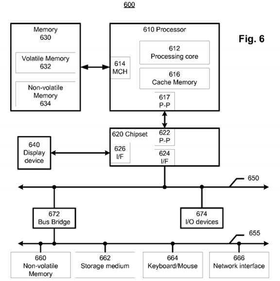
In one embodiment, the processor?610?has a processing core?612?to execute instructions of the system?600. In one embodiment, the processing core?612?includes, but is not limited to, pre-fetch logic to fetch instructions, decode logic to decode the instructions, execution logic to execute instructions and the like. In one embodiment, the processor?610?has a cache memory?616?to cache instructions and/or data of the system?600. In one embodiment, the cache stores the instructions to execute the method of?FIGS. 3-4?and?FIGS. 5A-B. In another embodiment of the invention, the cache memory616?includes level one, level two and level three, cache memory, or any other configuration of the cache memory within the processor?610.
The memory controller?101, which is also referred to as the memory control hub (MCH)?614, is operable to perform functions that enable the processor?610?to access and communicate with a memory?630?that includes a volatile memory?632and/or a non-volatile memory?634. The volatile memory?632?includes, but is not limited to, Synchronous Dynamic Random Access Memory (SDRAM), Dynamic Random Access Memory (DRAM), RAMBUS Dynamic Random Access Memory (RDRAM), and/or any other type of random access memory device. The non-volatile memory?634?includes, but is not limited to, NAND flash memory, phase change memory (PCM), read only memory (ROM), electrically erasable programmable read only memory (EEPROM), or any other type of non-volatile memory device.
The memory?630?stores information and instructions to be executed by the processor?610. In one embodiment, the memory630?may also store temporary variables or other intermediate information while the processor?610?is executing instructions. In one embodiment, the chipset?620?connects with the processor?610?via Point-to-Point (PtP) interfaces?617?and?622. In one embodiment, the chipset?620?enables the processor?610?to connect to other modules in the system?600. In one embodiment of the invention, the interfaces?617?and?622?operate in accordance with a PtP communication protocol such as the Intel? QuickPath Interconnect (QPI) or the like.
In one embodiment, the chipset?620?connects to a display device?640?via an interface?626. In one embodiment, the display device?640?includes, but is not limited to, liquid crystal display (LCD), cathode ray tube (CRT) display, or any other form of visual display device. In one embodiment of the invention, the processor?610?and the chipset?620?are merged into a SOC. In addition, the chipset?620?connects to one or more buses?650?and?655?that interconnect the various modules?674,?660,?662,664, and?666. In one embodiment, buses?650?and?655?may be interconnected together via a bus bridge?672?if there is a mismatch in bus speed or communication protocol. In one embodiment, the chipset?620?couples with, but is not limited to, a non-volatile memory?660, a mass storage device(s)?662, a keyboard/mouse?664, and a network interface?666?via an interface?624.
In one embodiment, the mass storage device?662?includes, but is not limited to, a solid state drive, a hard disk drive, an universal serial bus flash memory drive, or any other form of computer data storage medium. In one embodiment, the network interface?666?is implemented by any type of well known network interface standard including, but not limited to, an Ethernet interface, a universal serial bus (USB) interface, a Peripheral Component Interconnect (PCI) Express interface, a wireless interface and/or any other suitable type of interface. In one embodiment, the wireless interface operates in accordance with, but is not limited to, the IEEE 802.11 standard and its related family, Home Plug AV (HPAV), Ultra Wide Band (UWB), Bluetooth, WiMax, or any form of wireless communication protocol.
While the modules shown in?FIG. 6?are depicted as separate blocks within the system?600, the functions performed by some of these blocks may be integrated within a single semiconductor circuit or may be implemented using two or more separate integrated circuits. For example, although the cache memory?616?is depicted as a separate block within the processor?610, the cache memory?616?can be incorporated into the processor core?612?respectively. In one embodiment, the system?600may include more than one processor/processing core in another embodiment of the invention.
The term operable used herein means that the device, module, system, logic unit, protocol etc, is able to operate or is adapted to operate for its desired functionality when the device, module, system, or logic unit is in off-powered state.
Reference in the specification to "an embodiment," "one embodiment," "some embodiments," or "other embodiments" means that a particular feature, structure, or characteristic described in connection with the embodiments is included in at least some embodiments, but not necessarily all embodiments. The various appearances of "an embodiment," "one embodiment," or "some embodiments" are not necessarily all referring to the same embodiments. If the specification states a component, feature, structure, or characteristic "may," "might," or "could" be included, that particular component, feature, structure, or characteristic is not required to be included. If the specification or claim refers to "a" or "an" element, that does not mean there is only one of the elements. If the specification or claims refer to "an additional" element, that does not preclude there being more than one of the additional element.
While the invention has been described in conjunction with specific embodiments thereof, many alternatives, modifications and variations of such embodiments will be apparent to those of ordinary skill in the art in light of the foregoing description. For example, a memory module having an error pin other than a parity error pin (ALERT#) may be used for training (modifying) the C/A signal without initiating a JEDEC standardized initialization process. In one embodiment, the memory ranks?111?1-N?are not confined within a memory module.
The embodiments of the invention are intended to embrace all such alternatives, modifications, and variations as to fall within the broad scope of the appended claims.
SRC=https://www.google.com.hk/patents/US8533538
Method and apparatus for training a memory signal via an error signal of a memory,布布扣,bubuko.com
Method and apparatus for training a memory signal via an error signal of a memory
标签:des style blog http color os strong io
原文地址:http://www.cnblogs.com/coryxie/p/3889634.html