标签:fine sam rand one over font lin manager isa
In the PCB editor pin, pair and part swaps are performed by exchanging nets on component pads and corresponding copper. When the changes are merged into the schematics there are two ways that a pin swap can be handled, either by swapping the pins on the component symbol, or by swapping net labels on the wires attached to the pins. Each approach has its advantages and disadvantages.
Swapping the pins will always work on the schematic, but it may mean that this instance of the component symbol is no longer the same as it was defined in the library. In this situation it means the symbol cannot be updated from the library, and it also means that other instances of the same component in this design will have a different pin arrangement, a possible source of confusion to someone reading the schematic. This approach is ideal for simple components, such as a resistor arrays.
Performing the swap on the schematic by swapping net labels can only be done if the connectivity is established through the net labels, that is, if the pins are not hard-wired together. The advantage of this approach is that the component symbol does not change, and can be updated from the library at a later date. This approach is the best choice for a complex component, such as an FPGA, where physically moving two pins on the symbol could result in an I/O bank-based symbol presenting incorrectly.
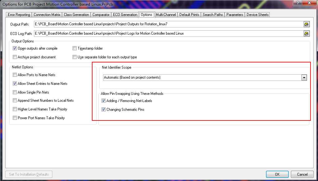
Selecting which of these two approaches is used is determined by the Allow Pin Swapping Using these Methods options in the Options for Project dialog, as shown in Figure 6.

Figure 6. Project options governing how pin swaps are updated in the schematic documents. Found in the menu item Project->Project Options under the Options tab.
----
step


Allow Pin Swapping Using these Methods options
标签:fine sam rand one over font lin manager isa
原文地址:http://www.cnblogs.com/qiyuexin/p/6783479.html