标签:des style blog http color io os ar strong
A data processing system includes a global promotion facility and a plurality of processors coupled by an interconnect. In response to execution of an acquisition instruction by a first processor among the plurality of processors, the first processor transmits an address-only operation on the interconnect to acquire a promotion bit field within the global promotion facility exclusive of at least a second processor among the plurality of processors. In response to receipt of a combined response for the address-only operation representing a collective response of others of the plurality of processors to the address-only operation, the first processor determines whether or not acquisition of the promotion bit field was successful by reference to the combined response.
The present invention relates in general to data processing and, in particular, to allocating and accessing resources within a data processing system. In at least one embodiment, the present invention relates still more particularly to a method and system for efficiently allocating and accessing promotion facilities, such as locks, in a data processing system.
In shared memory multiprocessor (MP) data processing systems, each of the multiple processors in the system may access and modify data stored in the shared memory. In order to synchronize access to a particular granule (e.g., cache line) of memory between multiple processors, programming models often require a processor to acquire a lock associated with the granule prior to modifying the granule and release the lock following the modification.
In a multiprocessor computer system, multiple processors may be independently attempting to acquire the same lock. In the event that a processor contending for a lock successfully acquires the lock, the cache line containing the lock is transmitted via the system bus from system memory or the cache hierarchy of another processor and loaded into the processor‘s cache hierarchy. Thus, the acquisition and release of locks in conventional data processing systems can be characterized as the movement of exclusively held cache lines between the data caches of various processors.
Lock acquisition and release is commonly facilitated utilizing special memory access instructions referred to as load-reserve and store-conditional instructions. In shared memory MP data processing systems that support load-reserve and store-conditional instructions, each processor within the system is equipped with a reservation register. When a processor executes a load-reserve to a memory granule, the processor loads some or all of the contents of the memory granule into one of the processor‘s internal registers and the address of the memory granule into the processor‘s reservation register. The requesting processor is then said to have a reservation with respect to the memory granule. The processor may then perform an atomic update to the reserved memory granule utilizing a store-conditional instruction.
When a processor executes a store-conditional to a memory granule for which the processor holds a reservation, the processor stores the contents of a designated register to the memory granule and then clears the reservation. If the processor does not have a reservation for the memory granule, the store-conditional instruction fails and the memory update is not performed. In general, the processor‘s reservation is cleared if a remote processor requests exclusive access to the memory granule for purposes of modifying it (the request is made visible to all processors on a shared bus) or the reserving processor executes a store-conditional instruction. If only one reservation is permitted per processor, a processor‘s current reservation will also be cleared if the processor executes a load-reserve to another memory granule.
A typical instruction sequence for lock acquisition and release utilizing load-reserve (lwarx) and store-conditional (stwcx) instructions is as fallows:
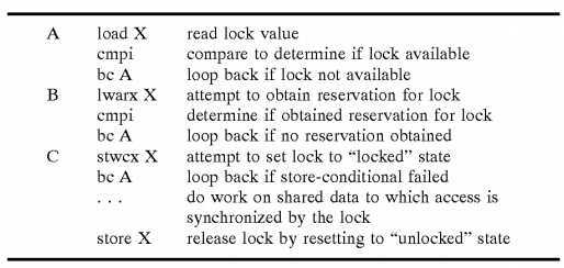
As indicated, the typical instruction sequence includes at least two separate branch "loops"—one (identified by "B") that is conditioned upon the processor obtaining a valid reservation for the lock through successful execution of the load-reserve instruction, and another (identified by "C") conditioned upon the processor successfully updating the lock to a "locked"state through execution of the store-conditional instruction while the processor has a valid reservation. The lock acquisition sequence may optionally include a third branch loop (identified by "A") in which the processor determines whether the lock is available prior to seeking a reservation for the lock.
This conventional lock acquisition sequence incurs high overhead not only because of its length but also because of the conditional nature of reservations. That is, a first processor may lose a reservation for a lock before successfully acquiring the lock (through execution of a store-conditional instruction) if a second processor stores to (or acquires ownership of) the lock first. Consequently, if a lock is highly contended, a processor may make a reservation for a lock and lose the reservation many times prior to successfully acquiring the lock through execution of a store-conditional instruction.
At least one processor manufacturer has tried to address this problem by implementing a "brute force" solution in which a processor executing a load-reserve instruction is granted exclusive access to the interconnect. That is, while the reservation is held by the processor, only the processor executing the load-reserve instruction is permitted to master operations on the interconnect, and all other processors are "locked out," not just from accessing a particular data granule, but from initiating any operation on the interconnect. Consequently, the processors locked out of the interconnect may stall for lack of data while the reservation is held. Obviously, this solution does not scale well, particularly for systems running code in which locks are highly contended.
The present invention recognizes that the conventional lock acquisition and release methodologies described above, although effective at synchronizing access by multiple processors to shared data, have a number of attendant shortcomings. First, conventional lock acquisition and release sequences that employ load-reserve and store-conditional instructions require the inclusion of special purpose reservation registers and reservation management circuitry within each processor, undesirably increasing processor size and complexity.
Second, as noted above, the typical lock acquisition and release sequence is inherently inefficient because of the conditional nature of reservations. If a lock is highly contended, multiple processors may gain and lose reservations for a lock many times before any processor is permitted to obtain the lock, update the lock to a "locked state," and do work on the data protected by the lock. As a result, overall system performance degrades.
Third, the lock acquisition and release methodologies outlined above do not scale well. For example, in the conventional lock acquisition instruction sequence, the overhead incurred in acquiring a lock increases with the scale of the data processing system. Thus, although it is more desirable in large-scale data processing systems having numerous processors to employ fine grain locks (i.e., a large number of locks that each protect a relatively small data granule) to enhance parallelism, the increasingly high lock acquisition overhead can force the adoption of coarser grain locks as system scale increases in order to reduce the percentage of processing time consumed by lock acquisition overhead. Such design compromises, though viewed as necessary, significantly diminish the amount of useful work that can be effectively distributed over multiple processors.
Fourth, because lock variables are conventionally treated as cacheable operand data, each load-type and store-type operation within the lock acquisition sequence triggers data cache directory snoops, coherency message traffic on the system bus, and other conventional operations dictated by the cache coherency protocol implemented by the data processing system. The present invention recognizes that these data-centric cache coherency operations, which consume limited system resources such as data cache snoop queues, bus bandwidth, etc., are not necessary because the data value of the lock itself is not required for or useful in performing the work on the data granule protected by the lock.
In view of the foregoing and other shortcomings of conventional techniques for acquiring and releasing locks in a data processing system, and more generally, of techniques for inter-component coordination and accessing memory-mapped resources, the present invention introduces, interalia, new methods and apparatus for allocating and accessing memory-mapped resources such as a global promotion facility that is not limited to, but can be advantageously employed as, as a lock facility.
In accordance with the present invention, a multiprocessor data processing system includes a plurality of processors coupled to an interconnect and to a memory including an promotion facility containing at least one promotion bit field. A first processor among the plurality of processors executes a load-type instruction to acquire a promotion bit field within the global promotion facility exclusive of at least a second processor among the plurality of processors. In response to execution of the load-type instruction, a register of the first processor receives a register bit field indicating whether or not the promotion bit field was acquired by execution of the load-type instruction. While the first processor holds the promotion bit field exclusive of the second processor, the second processor is permitted to initiate a request on the interconnect.
All objects, features, and advantages of the present invention will become apparent in the following detailed written description.
The novel features believed characteristic of the invention are set forth in the appended claims. The invention itself however, as well as a preferred mode of use, further objects and advantages thereof, will best be understood by reference to the following detailed description of an illustrative embodiment when read in conjunction with the accompanying drawings, wherein:
FIG. 1 depicts an illustrative embodiment of a multiprocessor data processing system in accordance with one embodiment of the present invention;
FIGS. 2A and 2B are more detailed block diagrams of two alternative embodiments of a processor core in accordance with the present invention; and
FIG. 3 is a more detailed block diagram of an embodiment of a promotion cache in accordance with the present invention;
FIG. 4 is a high level logical block diagram of a lock acquisition and release process in accordance with the present invention;
FIG. 5 is a timing diagram illustrating an address-only read transaction on a system interconnect that is utilized to acquire a lock in accordance with the present invention;
FIG. 6 is a software layer diagram of an exemplary software configuration of a multiprocessor data processing system in accordance with the present invention;
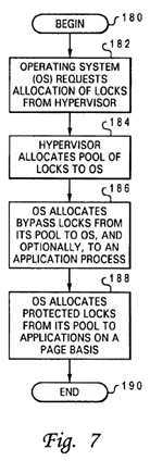
FIG. 7 depicts a high level logical diagram of a method by which memory-mapped resources, such as a global promotion facility, may be allocated by software; and
FIG. 8 illustrates a method by which access protection and address translation may be bypassed to accelerate accesses to particular memory-mapped resources, such as a global promotion facility.
As described above, the present invention recognizes that the shortcomings associated with conventional lock acquisition and release methodologies are at least partially attributable to the architectural definition of locks as operand data. That is, lock values are commonly accessed utilizing load-reserve and store-conditional atomic data access primitives, transmitted on the system interconnect during data tenures, stored within the operand data caches of processor cache hierarchies, and managed together with other operand data utilizing data cache coherency mechanisms.
To reduce or eliminate the problems attendant conventional lock acquisition and release methodologies, the present invention introduces a new class of information referred to herein as "promotion information." That is, rather than bifurcating the universe of addressable information subject to communication between components of a multiprocessor system into "instructions" and "operand data," the present invention introduces the additional information class of "promotion information," which includes locks. Such promotion information determines which components of a data processing system (e.g., processors, controllers, adapters, etc.) are authorized or permitted to perform particular activities associated with the promotion information. As will become apparent, software and hardware architectural enhancements are made to manage "promotion information" independently of operand data (as well as instructions), greatly simplifying and improving performance of the lock acquisition and release process.
With reference now to the figures and in particular with reference to FIG. 1, there is illustrated a high-level block diagram of a multiprocessor (MP) data processing system that supports improved management of locks and other promotion information in accordance with one embodiment of the present invention. As depicted, data processing system?8?includes multiple (e.g., 64) processing units?10?coupled for communication by a system interconnect?12. Each processing unit?10?is a single integrated circuit including interface logic?23?and one or more processor cores?14. In addition to the registers, instruction flow logic and execution units utilized to execute program instructions, each of processor cores?14?includes associated level one (L1) instruction and data caches?16?and?18, which temporarily buffer instructions and operand s data, respectively, that are likely to be accessed by the associated processor core?14.
As further illustrated in FIG. 1, the memory hierarchy of data processing system?8?also includes one or more system memories?26, which form the lowest level of volatile data storage in the memory hierarchy, and one or more lower levels of cache memory, such as on-chip level two (L2) caches?22, which are utilized to stage instructions and operand data from system memory?26?to processor cores?14. As understood by those skilled in the art, each succeeding lower level of the memory hierarchy is typically capable of storing a larger amount of data than higher levels, but at higher access latency.
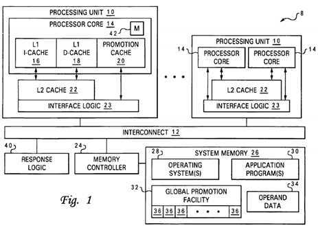
As shown, system memory?26, which is interfaced to interconnect?12?by memory controller?24, may store operand data?34and portions of one or more operating systems?28?and one or more application programs?30. In addition, system memory26?may include a global promotion facility?32?allocated (e.g., at boot time) by operating system(s)?28. Although illustrated as a facility within system memory, those skilled in the art will appreciate that global promotion facility?32?may alternatively be implemented within a system or bus controller, bus bridge, response logic, or other component of data processing system8.
Global promotion facility?32?includes a number (e.g., 1024) of individual promotion bits?36?that can be utilized to facilitate inter-component coordination, for example, regarding interrupts, locks, task scheduling, event detection, error conditions, permissions, etc. Although not limited to such application, some or all of promotion bits?36?may be allocated as locks and may be associated by operating system(s)?28?or application program(s)?30?with respective data granules of operand data34?to which access by multiple processor cores?14?is to be synchronized. For example, a promotion bit value of "1" may indicate that the lock is taken and the associated data granule is locked to access by processor cores?14?not holding the lock. Conversely, a promotion bit value of "0" may indicate that the lock is free and the associated data granule is unlocked. Memory controller?24?is preferably programmed to set a promotion bit promotion bit?36?(e.g., to "1") on a read access and to reset (e.g., to "0") a promotion bit on a write access.
To reduce access latency to global promotion facility?32, each processor core?14?may optionally be equipped with a promotion cache?20, which locally caches one or more promotion bits?36?accessed by the associated processor core?14, as described further below. Each promotion cache?20?can be implemented as a direct mapped or set associative cache, but is preferably implemented as a fully associative cache to enable promotion caches?20?to support greater or fewer promotion bits?36?(as determined by operating system(s)?28) without any hardware modification.
System interconnect?12, which can comprise one or more buses, a switch fabric, or other interconnect architecture, serves as a conduit for communication among the devices (e.g., processing units?10, memory controller?24, etc.) coupled to system interconnect?12. A typical transaction on system interconnect?12?begins with a request, which may include a transaction field indicating the type of transaction, one or more tags indicating the source and/or intended recipient(s) of the transaction, and an address and/or data. Each device connected to system interconnect?12?preferably snoops all relevant transactions on system interconnect?12?and, if appropriate, responds to the request with a snoop response. As discussed further below, such snoop responses are received and compiled by response logic?40, which provides a collective combined response indicating what action, if any, each snooper is to take in response to the request. These actions may include sourcing data on system interconnect?12, storing data provided by the requesting snooper, invalidating cached data, etc. Although illustrated separately, it should be understood that response logic?40?may alternatively be incorporated within a particular device (e.g., memory controller?24) or may be distributed among various devices (e.g., processing units?10) such that different devices (e.g., the masters of each transaction) compile the snoop responses to produce the combined response for different transactions.
Those skilled in the art will appreciate that data processing system?8?can include many additional unillustrated components, such as I/O adapters, interconnect bridges, non-volatile storage, ports for connection to networks or attached devices, etc. Because such additional components are not necessary for an understanding of the present invention, they are not illustrated in FIG. 1 or discussed further herein. It should also be understood, however, that the enhancements provided by the present invention are applicable to MP data processing systems of any architecture and are in no way limited to the generalized MP architecture illustrated in FIG.?1.
Referring now to FIG. 2A, there is depicted a more detailed block diagram of a first embodiment of a processor core?14?in accordance with the present invention. As shown, processor core?14?has an instruction sequencing unit?50?that fetches instructions for processing from L1 I-cache?16?utilizing real addresses obtained by the effective-to-real address translation (ERAT) performed by instruction (IMMU)?52. Of course, if the requested cache line of instructions does not reside in L1 I-cache?16, then ISU?50?requests the relevant cache line of instructions from L2 cache?22?via I-cache reload bus?54.
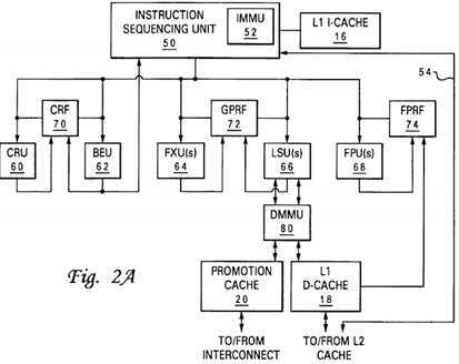
After instructions are fetched and preprocessing, if any, is performed, instructions are dispatched to execution units?60-68, possibly out-of-order, based upon instruction type. That is, condition-register-modifying instructions and branch instructions are dispatched to condition register unit (CRU)?60?and branch execution unit (BEU)?62, respectively, fixed-point and load/store instructions are dispatched to fixed-point unit(s) (FXUs)?64?and load-store unit(s) (LSUs)?66, respectively, and floating-point instructions are dispatched to floating-point unit(s) (FPUs)?68. After possible queuing and buffering, the dispatched instructions are executed opportunistically by execution units?60-68.
During execution within one of execution units?60-68, an instruction may receive input operands, if any, from one or more architected and/or rename registers within a register file?70-74?coupled to the execution unit. Data results of instruction execution (i.e., destination operands), if any, are similarly written to register files?70-74?by execution units?60-68. For example, FXU?64?receives input operands from and stores destination operands to general-purpose register file (GPRF)?72, FPU?68?receives input operands from and stores destination operands to floating-point register file (FPRF)?74, and LSU?66receives input operands from GPRF?72?and causes data to be transferred between L1 D-cache?18?and both GPRF?72?and FPRF?74. Similarly, when executing condition-register-modifying or condition-register-dependent instructions, CRU?90?and BEU?92?access control register file (CRF)?70, which in a preferred embodiment contains a condition register, link register, count register and rename registers of each. BEU?92?accesses the values of the condition, link and count registers to resolve conditional branches to obtain a path address, which BEU?62?supplies to instruction sequencing unit?50?to initiate instruction fetching along the indicated path. After an execution unit finishes execution of an instruction, the execution unit notifies instruction sequencing unit?50, which schedules completion of instructions in program order.
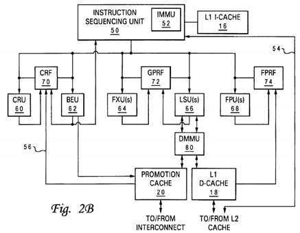
In the processor architecture depicted generally in FIG. 2A, various execution units (and therefore differing instruction sequences) may be employed to access promotion cache?20?to acquire and release locks and perform other inter-component coordination functions. For example, FIG. 2A illustrates an implementation in which LSU?66?accesses promotion bits?36?(within optional promotion cache?20?or from global promotion facility?32) in response to special-purpose or general-purpose load and store instructions. FIG. 2B depicts an alternative second embodiment in which BEU?62?sets a promotion bit?36?(e.g., to acquire a lock) within optional promotion cache?20?or within global promotion facility?32?in response to a special branch instruction, and LSU?66?resets a promotion bit?36?(e.g., to release a lock) in response to a store instruction. Of these and other design options within the scope of the present invention, differing designs may be preferable, depending upon implementation-specific details (e.g., gate counts, layout and routing efficiencies, instruction set architecture, etc.) known to those skilled in the art.
With reference now to FIG. 3, there is illustrated a more detailed block diagram of a promotion cache?20?of a processor core?14?in accordance with a preferred embodiment of the present invention. As shown, promotion cache?20?includes a fully associative cache array?90?containing one or more entries?92. Each entry?92?within cache array?90?includes a valid bit field100, a bit ID field?102, and a bit value field?104?indicating whether the associated processor core?14?currently holds the promotion bit?36?(e.g., lock) identified within bit ID field?102. For example, a bit value of "1" indicates that the associated processor core?14?holds the lock, and a bit value of "0" indicates that the lock is free.
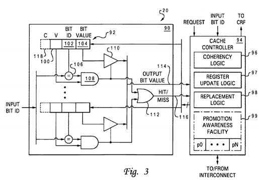
Associated with each entry?92?is an access circuit including a comparator?106, AND gate?108, and a buffer?110. Comparator?106?compares an input bit ID received from the associated processor core?14?or system interconnect?12?with the bit ID stored within the associated entry?92?and outputs a 1-bit hit/miss indication indicating whether the input bit ID and stored bit ID match. This hit/miss signal is qualified by AND gate?108?with the state of valid field?100, and if the qualified signal indicates a hit, buffer?110?outputs the bit value contained in bit value field?104. The qualified hit/miss signals output by all of AND gates?108?are received as inputs by OR gate?112, which outputs a 1-bit collective hit/miss indication?116. Hit/miss indication?116?and the output bit value?114, if any, are received by a cache controller?94.
Cache controller?94?comprises a collection of logic that manages access to and updates and coherency of cache array?90. In the illustrated embodiment, cache controller?94?includes coherency logic?96, register update logic?97, replacement logic98, and an optional promotion awareness facility?99.
Coherency logic?96?maintains coherency between the contents of promotion caches?20?and the global promotion facility?32within system memory?26. Numerous implementations of coherency logic?96?are possible, of which various ones may be preferable for different systems depending upon desired complexity, performance, number of frequently contended locks, etc.
In general, coherency logic?96?maintains coherency by managing the states of valid bit fields?100?and/or bit value fields?104in response to requests by both the local processor core?14?and remote processor cores?14. In an exemplary implementation in which no additional coherency field?118?is implemented, coherency logic?96?permits only one promotion cache?20?at a time to have a valid entry?92?containing a particular promotion bit?36?from global promotion facility?32. Table I provides a summary of the operations of coherency logic?96?according to this exemplary implementation.
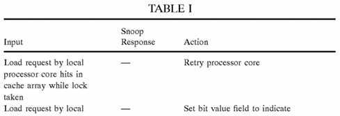
It should be noted that in the implementation summarized in Table I (as well as other implementations) writeback of the state of a promotion bit?36?to global promotion facility?32?to inform global promotion facility?32?of the release of a lock can optionally be delayed from the time of release until deallocation of the promotion bit?36?by all promotion caches?20. During the period that global promotion facility?32?is not synchronized with promotion caches?20?(e.g., global promotion facility?32indicates that a lock has been acquired by a processor core?14?while in fact the lock is indicated within a promotion cache20?as free), memory controller?24?will respond to a read request targeting the lock with a snoop response indicating that a lock is taken. Processor cores?14, on the other hand, will provide either Null or Intervention snoop response (i.e., no processor core?14?provides a Retry snoop response). In response to these snoop responses, response logic?40?will provide a combined response indicating that the lock acquisition request is granted to the requesting processor core?14.
In other embodiments of coherency logic?96, each promotion cache?20?may permit promotion bits?36?to be cached concurrently within the promotion caches?20?of multiple processor cores?14. Such embodiments may decrease average lock acquisition overhead, particularly for highly contended locks, but concomitantly increase cache complexity. For example, each entry?92?of a promotion cache?20?is equipped with a coherency field?118?in addition to (or in lieu of) valid bit field?100to track the coherency state of promotion bit?36?cached in that entry?92, and coherency logic?99?additionally implements a coherency protocol, such as the well known Modified, Exclusive, Shared, Invalid (MESI) cache coherency protocol or a variant thereof.
Cache controller?94?also includes register update logic?97?that updates one or more selected registers within processor core?14?in response to an access to promotion cache?20. For example, register update logic?97?may update a general-purpose register within GPRF?72?with the lock value (e.g., 0 or 1) in response to lock acquisition or release instructions targeting global promotion facility?32. Alternatively or additionally, as illustrated in FIG. 2B at reference numeral?56, register update logic?97?may update one or registers within CRF?70?(e.g., a link register, condition register, or special purpose lock register) in response to lock acquisition and release instructions targeting global promotion facility?32.
Cache controller?94?further includes replacement logic?98?that replaces a selected entry?92?of cache array?90?in response to an access request missing in promotion cache?20. Replacement logic?98?may implement a conventional cache replacement algorithm such as Least Recently Used (LRU) or Most Recently Used (MRU), or alternatively, may replace promotion bits36?based upon individual or group priority, which can be dynamically determined (e.g., by operating system(s)?28) or statically determined at startup. In this second implementation, higher priority locks are advantageously prevented from being displaced by lower priority locks, further improving lock acquisition efficiency. In implementations in which the locks are managed by replacement logic?98?in various priority groups in which the locks of each group share the same priority level, cache array?90?is effectively partitioned into multiple independent caches (e.g., at least one higher priority cache and at least one lower priority cache) by the groupings. Within such partitions, locks sharing a same priority level may be selected by replacement logic?98?for replacement according to access order (e.g., LRU or MRU).
Optional promotion awareness facility?99?provides further enhancements to the method by which the release and/or cache deallocation (victimization) of promotion bits is handled. In particular, promotion awareness facility?99?may track the particular promotion bit?36, if any, that has been most recently requested (or most recently unsuccessfully requested based upon the CR value) by each other processing unit?10?or other component (indicated in FIG. 3 as p0-pN) based upon address-only requests snooped on interconnect?12. Alternatively or additionally, promotion awareness facility may provide a table indicating, for each promotion bit?36, the processing unit?10?(or other component) that has the oldest outstanding (i.e., unsatisfied) or highest priority request for that promotion bit?36. If desired, the amount of information promotion awareness facility?99?stores regarding snooped requests for promotion bits?36?can be limited by recording the processing unit?10?(or other component) that is the oldest unsatisfied requester (or highest priority requester) of only the promotion bits?36?that are cached within the associated promotion cache?20?or held by the associated processor core?14.
If replacement logic?98?selects a promotion bit for deallocation from cache array?90?that is indicated by promotion awareness facility?99?as requested by a processing unit?10, cache controller?94?can source (push) the promotion bit?36?to the indicated processing unit?10?without receiving another request by transmitting an unsolicited address-only push operation on interconnect?12. If promotion awareness facility?99?indicates the deallocated promotion bit?36?is concurrently desired by multiple processing units?10?(as is often the case for highly contended locks), replacement logic?98?preferably pushes the deallocated promotion bit?36?to the processing unit?10?that has the oldest outstanding (or highest priority) request for the promotion bit?36. The push operation can alternatively be issued by cache controller?94?in response to release of the promotion bit?36?rather than waiting for deallocation from promotion cache?20?if promotion awareness facility?99?indicates that another processing unit?10?(or other component) has requested the promotion bit?36?or has an unsatisfied outstanding request for the promotion bit?36. If for some reason the push operation fails (e.g., the target processing unit?10?has no snoop queues available), memory controller?24?preferably updates global promotion facility?32?to indicate that the deallocated promotion bit?36?is available and assumes "ownership" of the deallocated promotion bit?36.
As address-only promotion push operations and address-only promotion request operations are snooped, the cache controller?94?in each cache may clear the entry in its promotion awareness facility?99?corresponding to the target processing unit?10?of the push operation. In addition, if a processing unit?10?no longer wants to acquire a previously requested promotion bit?36?(e.g., the processing unit?10?unsuccessfully requested the promotion bit?36?a predetermined number of times and then switched processes), the processing unit?10?can transmit an address-only operation on interconnect?12?requesting that other processing units?10?clear the corresponding entry from their promotion awareness facilities?99. An entry within promotion awareness facility?99?for a particular processing unit?10?is also updated to a new value in response to snooping a request by the particular processor?10?for a different promotion bit?36.
It should be noted that the implementation of a promotion awareness facility?99?does not require the implementation of a promotion cache?20?and may be implemented within processing units?10?not having a promotion cache?20. Moreover, a promotion awareness facility?99?in accordance with the present invention may further be employed even in otherwise conventional data processing systems that employ data cache lines as locks. It should further be recognized that the level of precision with respect to the communication and management of promotion requests can vary between implementations, based upon interconnect topologies, protocols, and other factors.
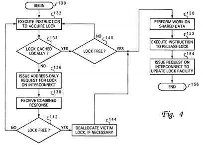
Referring now to FIG. 4, there is depicted a high level logical flowchart of a method by which a processor core?14?acquires a lock associated with a shared data granule and thereafter releases the lock in accordance with the present invention. As illustrated, the process begins at block?130?and thereafter proceeds to block?132, which depicts a processor core?14executing a lock acquisition instruction to acquire a lock for a particular data granule.
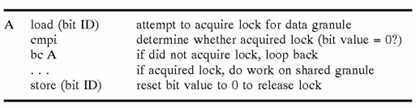
For example, in a first embodiment, the instruction executed to acquire a lock may be a general-purpose or special load instruction targeting the base address of global promotion facility?32, where the load instruction identifies with an operand the particular promotion bit?36?utilized for the lock. In this first embodiment, the lock acquisition and release instruction sequence can be represented as follows:
In the processor core embodiment illustrated in FIG. 2A, instruction sequencing unit?50?dispatches the load instruction utilized to acquire the lock to an LSU?66?for execution. LSU?66?executes the load instruction by calculating the effective or real address of global promotion facility?32. This request address is then translated, if necessary, to a real address by DMMU?80?and, based upon this translation (e.g., through a table lookup in a block address table (BAT)), presented to promotion cache?20?rather than L1 data cache?18?(if a promotion cache?20?is implemented).
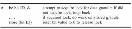
In a second embodiment, the instruction sequence utilized to acquire a lock may be further shortened by utilizing as the lock acquisition instruction a special branch instruction identifying with an operand the particular promotion bit?36?utilized for the lock. In this second embodiment, the lock acquisition and release sequence can be represented as follows:
In the processor core embodiment illustrated in FIG. 2B, instruction sequencing unit?50?dispatches the conditional branch instruction utilized to acquire the lock to BEU?62?for execution. BEU?62?executes the branch instruction by issuing to promotion cache?20?an access request specifying the bit ID.
As illustrated at block?134?of FIG. 4, in response to an access request, cache controller?94?determines by reference to the hit/miss indication?116?and output bit value?114?provided by cache array?90?whether or not the promotion bit?36?utilized for the lock is cached within promotion cache?20. If so, register update logic?97?updates a register within processor core?14(e.g., a general-purpose register within GPRF?72?or selected register within CRF?70) with the bit value of the lock. A determination is then made at block?140?whether the lock is free, for example, by reference to the bit value of a register within GPRF?72?or CRF?70. If not, the process returns to block?132, which has been described. If, however, the lock is successfully acquired, the process proceeds from block?140?to block?150?and following blocks, which are described below.
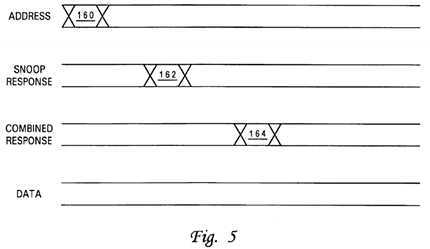
Returning to block?134, if the processor core‘s access request misses in promotion cache?20?(or if no promotion cache?20?is implemented), the process proceeds to block?136, which depicts processor core?14?(and in embodiments including promotion cache?20, the cache controller?94) issuing on interconnect?12?(via interface logic?23) an address-only read request targeting the lock, as depicted in FIG. 5 at reference numeral?160. In response to snooping the address-only read request, devices (e.g., processing units?10, memory controller?24, etc.) coupled to interconnect?12?provide snoop responses, illustrated collectively at reference numeral?162?of FIG.?5. As discussed above, response logic?40?compiles these snoop responses?162?to produce a single combined response (CR)?164, which represents a collective response of the snooping devices providing snoop responses. Combined response?164?is provided to at least the processing unit?10issuing the read request targeting the lock as indicated at block?138?of FIG. 4, and more preferably, to all agents snooping the transaction.
As shown in FIG. 5, in contrast to conventional methods of lock acquisition, address-only read request?160?does not have any associated data tenure on system interconnect?12?that provides the lock value. Instead, combined response?164indicates to the requesting processor core?14?whether or not the lock was successfully acquired. For example, in the embodiment described above, a Retry combined response generally indicates that the lock is currently taken by another processor core?14, and any other combined response indicates that the lock is available to the requesting processor core14. It is preferable in determining the combined response if the highest point of promotion "ownership" (i.e., a promotion cache?20?if the promotion bit is cached and otherwise global promotion facility?36) can always grant a promotion bit?36?to a requester regardless of Retry responses of individual snoopers. As noted above, cache controller?94?allocates an entry?92within cache array?90?in response to a combined response indicating acquisition of the lock.
The process proceeds from block?138?through block?142?and returns to block?132?in the event that the combined response does not indicate acquisition of the lock was successful. However, in the event that lock acquisition was successful, the process proceeds to block?144, which illustrates deallocation of a selected victim promotion bit from promotion cache?20, if necessary. As noted above, the deallocated promotion bit?36?may be returned to global promotion facility?32?or pushed directly to another processing unit?10?(or other component).
Following block?144, the process passes to block?150, which illustrates the processor core?14?processing (e.g., modifying) the shared data associated with the lock, for example, through execution of instructions by FXUs?64?and FPUs?68. In contrast to the prior art systems noted above that lock the system interconnect to processors not holding a reservation, processor cores?14?of data processing system?8?can master requests on system interconnect?12?and acquire locks for other data granules while the processor core?14?holds the lock.
After completing processing on the shared data granule associated with the lock, processor core?14?executes a lock release instruction (e.g., a store instruction) to release the lock, as shown at block?152. Thereafter, the processor core?14that held the lock (or another processor core?14?that later acquires the lock) eventually issues a write request on interconnect?12?to update global promotion facility?32?to indicate the release of the lock. Thereafter, the process terminates at block?156.
Further refinements to the foregoing method and apparatus for lock acquisition may be advantageous for certain applications. First, it may be desirable to aggregate multiple promotion bits?36?(e.g., locks) so that all of the promotion bits36?are atomically obtained by one processor core?14?in response to a single lock acquisition instruction or the acquisition attempt fails for all of the promotion bits?36.
Several embodiments of aggregated promotion bits?36?are possible. For example, if load-reserve and store-conditional instructions are employed in a lock acquisition sequence, the store-conditional instruction may be implemented with multiple operands, such that the store-conditional instruction completes successfully (i.e., updates the lock value) only if the processor core holds valid reservations for all of the locks specified by the multiple operands of the store-conditional instruction. Thus, the conventional lock acquisition sequence set forth above may be rewritten as:
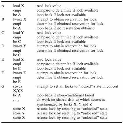
Similarly, the load or branch lock acquisition instruction executed by a processor core?14?to acquire a lock and/or the interconnect operation utilized to convey a lock request can be implemented with multiple operands (or a bit mask) to indicate multiple locks that must be obtained in concert. To limit the size of the operand field, it may be desirable in some embodiments to simply specify a group of promotion bits?36?grouped by software (e.g., group?1, which is specified by software to include promotion bits?3,?27,?532?and?1000). If all the specified promotion bits?36?are free, all of the specified promotion bits?36?are acquired by the processor core?14?and set to "1"; otherwise, the lock acquisition attempt fails for all of the specified promotion bits?36.
Of course, bundling or aggregating promotion bits?36?in this manner reduces the success rate of lock acquisition requests in that all locks must be available at the same time. However, for many types of workloads, performance is nevertheless increased by bundling locks since individual locks within a group of locks needed to perform a particular activity are not individually held until all of the locks in the group become available.
Advantage can be taken of implementation of global promotion facility?32?as a software-managed resource to achieve flexibility in addressing and security. Software could additionally partition global promotion facility?32?or define affinity between processor cores?14?and promotion bits?36?so that only particular processor cores?14?can acquire certain promotion bits?36. These concepts can best be appreciated by reference to FIGS. 6-8.
Referring now to FIG. 6, there is illustrated a software layer diagram of an exemplary software configuration of data processing system?8?of FIG.?1. As illustrated, the software configuration has at its lowest level an operating system supervisor (or hypervisor)?170?that allocates resources among one or more operating systems?28?concurrently executing within data processing system?8. The resources allocated to each instance of an operating system?28?are referred to as a partition. Thus, for example, hypervisor?170?may allocate two processing units?10?to the partition of operating system?28?a, four processing units?10?to the partition of operating system?28?b, and certain ranges of real and effective address spaces to each partition. Included within the resources allocated to each partition by hypervisor?170?are promotion bits?36?within global promotion facility?32, as discussed further below with reference to FIG.?7.
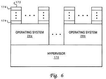
Running above hypervisor?170?are operating systems?28?and application programs?172. As well understood by those skilled in the art, each operating systems?28?allocates resources from the pool of resources allocated to it by hypervisor?170?to various operating system processes and applications?172, independently controls the operation of the hardware allocated to its partition, and provides various application programing interfaces (API) through which operating system services can be accessed by its application programs?172. Application programs?172, which can be programmed to perform any of a wide variety of computational, control, communication, data management and presentation functions, comprise a number of user-level processes?174.
With reference now to FIG. 7, there is depicted a high level logical flowchart of a method by which memory-mapped resources, such as promotion bits?36?within a global promotion facility?32, may be allocated. The process depicted in FIG. 7, which is performed individually by each operating system?28, assumes (but does not require) the exemplary software configuration illustrated in FIG.?6.
As shown, the process begins at block?180?after booting of data processing system?8?and then proceeds to block?182, which illustrates an operating system?28?requesting an allocation of locks from hypervisor?170. The request may specify, for example, a requested number of locks. As shown at block?184, in response to the request (and requests from other operating systems?28), hypervisor?170?allocates a pool of locks (i.e., particular promotion bits?36) to the operating system28?from global promotion facility?32. Hypervisor?170?may allocate all of promotion bits?36?as locks, or as noted above, may allocate some of promotion bits?36?as locks and reserve other promotion bits?36?for other types of inter-component coordination.
The process proceeds from block?184?to blocks?186?and?188, which illustrates operating system?28?allocating locks from its pool. In accordance with a preferred embodiment of the present invention, operating system?28?can allocate at least two types of locks from its pool: bypass locks and protected locks. Bypass locks are herein defined as locks that can be accessed by a process without implementation of access protection, thus bypassing the access protection typically performed by address translation facilities. Conversely, protected locks are herein defined as locks that can be accessed by a process only in conjunction with access protection.
As shown in block?186, operating system?28?allocates bypass locks from its pool to operating system (e.g., kernel) processes, and optionally, to applications?172. The bypass locks allocated by an operating system?28?to applications?172are each preferably allocated to a single process (e.g., the application root process) per application to promote well-behaved applications. Operating system?28?also allocates protected locks from its pool to applications?172, preferably as a fixed number of protected locks per page of non-real (e.g., virtual) address space allocated to the application?172. The number of locks per virtual memory page can be determined by operating system?28, or alternatively, by mode bits?42?(see FIG. 1) within a processor core?14?to permit hardware to optimize lock allocation. As will be appreciated by those skilled in the art, it is preferable for multiple locks to be allocated on each page to avoid unnecessarily rolling the translation lookaside buffer (TLB) as different locks are accessed. Following allocation of the bypass locks and protected locks, the process illustrated in FIG. 7 terminates at block?190.
Referring now to FIG. 8, there is illustrated a more detailed block diagram of DMMU?80?of FIGS. 2A and 2B, which depicts the manner in which access requests for memory-mapped resources, such as global promotion facility?32, are accelerated when access protection is bypassed. As shown, DMMU?80?includes bypass logic?212?coupled to address translation facilities that include translation lookaside buffer (TLB)?214?and a block address table (BAT)?216. As is well known to those skilled in the art, TLB?214?is a cache of recently referenced page frame table (PFT) entries that are accessed to translate non-real (e.g., effective or virtual) addresses within uniform pages of a virtual address space into real addresses. BAT?216similarly translates non-real addresses into real addresses by reference to cached table entries, but is utilized to translate non-real addresses falling within non-uniform (rather than uniform) blocks of the virtual address space. Both of TLB?214?and BAT?216?provide access protection through access protection bits (often referred to as?WIMG?bits for PowerPC-based processors) within the PFT entries.
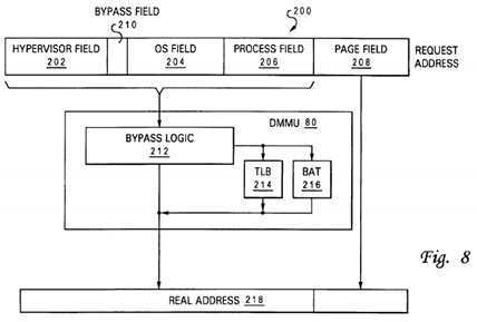
As shown in FIG. 8, DMMU?80?receives a request address?200?to access a memory-mapped resource from LSU?66(and/or BEU?62?in the embodiment of FIG.?2B). Request address?200?includes a lower order portion containing page field208?and a higher order portion including hypervisor field?202, OS field?204?and process field?206. Hypervisor field?202, OS field?204?and process field?206?are generally determined by hypervisor?170, an operating system?28, and a process (e.g., application process?174) according to the real and/or virtual address spaces allocated to and controlled by each piece of software. Within OS field?204, a bypass field?210?is provided that can be set to a bypass state (e.g. a "1") by any application or operating system process that has been allocated a bypass lock when request address?200?specifies a bypass lock allocated to that process.
In response to receipt of request address?200, bypass logic?212?determines by reference to bypass field?210?whether or not the access request should be permitted to bypass the access protection provided by TLB?214?and BAT?216. If so, request address?200?can be transmitted as real address?218?directly to the memory-mapped resource (e.g., promotion cache?20?or system memory?26) to initiate an access. Thus, request addresses?200?having bypass field?210?set to the bypass state bypass both address translation and access protection, reducing access latency for the associated access requests by at least one (and typically more) processor cycles. In the event that bypass field?210?of a request address?200is not set to the bypass state, signifying the need for address translation and access protection, the higher order portion of request address?200?comprising hypervisor field?202, OS field?204?and process field?206?is translated by reference to TLB214?or BAT?216?to obtain the higher order portion of real address?218. Concurrent with the address translation, TLB?214?or BAT?216?implements access protection to ensure that the process issuing the access request is permitted to access to the requested lock. Thereafter, DMMU?80?transmits real address?218?to initiate access to the memory-mapped resource.
Although FIGS. 7-8 have been described with specific reference to locks, and more generally, with respect to memory-mapped global promotion facilities, it should be appreciated that the techniques described with reference to FIGS. 7 and 8 can generally be applied to accelerate access to any memory-mapped facility whether or not it resides within a memory device.
While the invention has been particularly shown and described with reference to a preferred embodiment, it will be understood by those skilled in the art that various changes in form and detail may be made therein without departing from the spirit and scope of the invention. For example, although the present invention has been described with reference to particular embodiments in which promotion bits are employed as locks, it should be understood that the present invention is not limited to such embodiments, but is instead broadly applicable to inter-component coordination in a multiprocessor data processing system. In addition, although in some instances, the description of the present invention assumes that certain promotion bits must be held exclusively (e.g., certain locks), it should be understood that the notion of promotion includes the ability of multiple components to concurrently hold a particular promotion bit and therefore be able to perform activities associated with the promotion bit. Furthermore, the exclusivity of selected promotion bits can localized, for example, in a particular cluster of processing units or on a particular one of a plurality of hierarchical buses.
SRC=https://www.google.com.hk/patents/US6829698
标签:des style blog http color io os ar strong
原文地址:http://www.cnblogs.com/coryxie/p/3989426.html