标签:
0xWS2812 pronounced "hex-WS2812"
This code aims at providing a basic interface to the WS2812(B) individually addressable RGB LEDs by WorldSemi.
The code outputs 16 parallel data streams to 16 parallel strings of LEDs. This allows the MCU to drive a large number of LEDs rather memory efficient, although RAM size is still the limiting factor for the number of LEDs that can be driven.
The number of LEDs that can be driven by this library can be approximated by the following formula (it won‘t be exactly that many as the library needs some RAM, too): Number of LEDs = (RAM size in bytes / 48) * 16
Calm your finite state machines.
This code is a work in progress and I admit that in it‘s current form it‘s a bit of a hassle adapting it to different MCUs. I will get around to working more on this when I have time as I‘m also busy with school finals. If you find a bug please report it and if you can and are willing to, provide a fix.
At some point this might actually become a full grown library that supports STM32F100, STM32F4 etc.
Due to the non-standard NRZ protocol used to control these LEDs the correct timing of the data stream is very important and is not easily achievable with standard MCU peripherals like SPI/USART/I2C.
The approach used here is similar to the approach of the OctoWS2812 library for the Teensy.
This library makes use of the output compare features of the STM32s General Purpose Timer and the DMA (Direct Memory Access) controller. The DMA allows to transfer data from memory to a peripheral register in this case a GPIO port quickly without the CPU being involved. Therefore the CPU can already prepare the next frame to be sent while the current frame is still being transmitted.
The idea to create 16 parallel 800kBit/s data streams is the following:
Use 2 compare modules to create DMA requests at the low bit time (350ns) and the high bit time (700ns)
This creates a stream of pulses with a pulse period of 1.25us and a pulse width of either 350ns or 700ns depending on the bit value the pulse represents.
Transferring the data via DMA to the GPIO port means that per 16 LEDs one half word (two bytes) is needed per bit. At 24 bits per LED that makes 24 half words (48 bytes) per 16 LEDs.
The frame buffer is transmitted MSBit first in the order G-R-B.
Currently you have to fill the frame buffer with 24 bytes per 16 LEDs and then call the WS2812_sendbuf(24*#LEDs).
This code is licensed under the MIT License, see LICENSE for more info.
/* 0xWS2812 16-Channel WS2812 interface library
 *
 * Copyright (c) 2014 Elia Ritterbusch, http://eliaselectronics.com
 *
 * Permission is hereby granted, free of charge, to any person obtaining a copy
 * of this software and associated documentation files (the "Software"), to deal
 * in the Software without restriction, including without limitation the rights
 * to use, copy, modify, merge, publish, distribute, sublicense, and/or sell
 * copies of the Software, and to permit persons to whom the Software is
 * furnished to do so, subject to the following conditions:
 *
 * The above copyright notice and this permission notice shall be included in
 * all copies or substantial portions of the Software.
 *
 * THE SOFTWARE IS PROVIDED "AS IS", WITHOUT WARRANTY OF ANY KIND, EXPRESS OR
 * IMPLIED, INCLUDING BUT NOT LIMITED TO THE WARRANTIES OF MERCHANTABILITY,
 * FITNESS FOR A PARTICULAR PURPOSE AND NONINFRINGEMENT. IN NO EVENT SHALL THE
 * AUTHORS OR COPYRIGHT HOLDERS BE LIABLE FOR ANY CLAIM, DAMAGES OR OTHER
 * LIABILITY, WHETHER IN AN ACTION OF CONTRACT, TORT OR OTHERWISE, ARISING FROM,
 * OUT OF OR IN CONNECTION WITH THE SOFTWARE OR THE USE OR OTHER DEALINGS IN
 * THE SOFTWARE.
 */

#include <stm32f10x.h>

/* this define sets the number of TIM2 overflows to append to the data frame for the LEDs to load the received data into their registers */
#define WS2812_DEADPERIOD 19

uint16_t WS2812_IO_High = 0xFFFF;
uint16_t WS2812_IO_Low = 0x0000;

volatile uint8_t WS2812_TC = 1;
volatile uint8_t TIM2_overflows = 0;

/* WS2812 framebuffer buffersize = (#LEDs / 16) * 24 */
uint16_t WS2812_IO_framedata[ 48 ];

/* Array defining 12 color triplets to be displayed */
uint8_t colors[ 12 ][ 3 ] =
{
{ 0xFF, 0x00, 0x00 },
{ 0xFF, 0x80, 0x00 },
{ 0xFF, 0xFF, 0x00 },
{ 0x80, 0xFF, 0x00 },
{ 0x00, 0xFF, 0x00 },
{ 0x00, 0xFF, 0x80 },
{ 0x00, 0xFF, 0xFF },
{ 0x00, 0x80, 0xFF },
{ 0x00, 0x00, 0xFF },
{ 0x80, 0x00, 0xFF },
{ 0xFF, 0x00, 0xFF },
{ 0xFF, 0x00, 0x80 } };

/* simple delay counter to waste time, don‘t rely on for accurate timing */
void Delay(__IO uint32_t nCount)
{
  while(nCount--)
  {
  }
}

void GPIO_init( void )
{
  GPIO_InitTypeDef GPIO_InitStructure;
  // GPIOA Periph clock enable
  RCC_APB2PeriphClockCmd( RCC_APB2Periph_GPIOA, ENABLE );
  // GPIOA pins WS2812 data outputs
  GPIO_InitStructure.GPIO_Pin = 0xFFFF;
  GPIO_InitStructure.GPIO_Mode = GPIO_Mode_Out_PP;
  GPIO_InitStructure.GPIO_Speed = GPIO_Speed_50MHz;
  GPIO_Init( GPIOA, &GPIO_InitStructure );
}

void TIM2_init( void )
{
  TIM_TimeBaseInitTypeDef TIM_TimeBaseStructure;
  TIM_OCInitTypeDef TIM_OCInitStructure;
  NVIC_InitTypeDef NVIC_InitStructure;

  uint16_t PrescalerValue;

  // TIM2 Periph clock enable
  RCC_APB1PeriphClockCmd( RCC_APB1Periph_TIM2, ENABLE );

  PrescalerValue = (uint16_t) ( SystemCoreClock / 24000000 ) - 1;
  /* Time base configuration */
  TIM_TimeBaseStructure.TIM_Period = 29; // 800kHz
  TIM_TimeBaseStructure.TIM_Prescaler = PrescalerValue;
  TIM_TimeBaseStructure.TIM_ClockDivision = 0;
  TIM_TimeBaseStructure.TIM_CounterMode = TIM_CounterMode_Up;
  TIM_TimeBaseInit( TIM2, &TIM_TimeBaseStructure );

  TIM_ARRPreloadConfig( TIM2, DISABLE );

  /* Timing Mode configuration: Channel 1 */
  TIM_OCInitStructure.TIM_OCMode = TIM_OCMode_Timing;
  TIM_OCInitStructure.TIM_OutputState = TIM_OutputState_Disable;
  TIM_OCInitStructure.TIM_Pulse = 8;
  TIM_OC1Init( TIM2, &TIM_OCInitStructure );
  TIM_OC1PreloadConfig( TIM2, TIM_OCPreload_Disable );

  /* Timing Mode configuration: Channel 2 */
  TIM_OCInitStructure.TIM_OCMode = TIM_OCMode_PWM1;
  TIM_OCInitStructure.TIM_OutputState = TIM_OutputState_Disable;
  TIM_OCInitStructure.TIM_Pulse = 17;
  TIM_OC2Init( TIM2, &TIM_OCInitStructure );
  TIM_OC2PreloadConfig( TIM2, TIM_OCPreload_Disable );

  /* configure TIM2 interrupt */
  NVIC_InitStructure.NVIC_IRQChannel = TIM2_IRQn;
  NVIC_InitStructure.NVIC_IRQChannelPreemptionPriority = 0;
  NVIC_InitStructure.NVIC_IRQChannelSubPriority = 2;
  NVIC_InitStructure.NVIC_IRQChannelCmd = ENABLE;
  NVIC_Init( &NVIC_InitStructure );
}

void DMA_init( void )
{
  DMA_InitTypeDef DMA_InitStructure;
  NVIC_InitTypeDef NVIC_InitStructure;

  RCC_AHBPeriphClockCmd( RCC_AHBPeriph_DMA1, ENABLE );

  // TIM2 Update event
  /* DMA1 Channel2 configuration ----------------------------------------------*/
  DMA_DeInit( DMA1_Channel2 );
  DMA_InitStructure.DMA_PeripheralBaseAddr = (uint32_t) &GPIOA->ODR;
  DMA_InitStructure.DMA_MemoryBaseAddr = (uint32_t) WS2812_IO_High;
  DMA_InitStructure.DMA_DIR = DMA_DIR_PeripheralDST;
  DMA_InitStructure.DMA_BufferSize = 0;
  DMA_InitStructure.DMA_PeripheralInc = DMA_PeripheralInc_Disable;
  DMA_InitStructure.DMA_MemoryInc = DMA_MemoryInc_Disable;
  DMA_InitStructure.DMA_PeripheralDataSize = DMA_PeripheralDataSize_Word;
  DMA_InitStructure.DMA_MemoryDataSize = DMA_MemoryDataSize_HalfWord;
  DMA_InitStructure.DMA_Mode = DMA_Mode_Normal;
  DMA_InitStructure.DMA_Priority = DMA_Priority_High;
  DMA_InitStructure.DMA_M2M = DMA_M2M_Disable;
  DMA_Init( DMA1_Channel2, &DMA_InitStructure );

  // TIM2 CC1 event
  /* DMA1 Channel5 configuration ----------------------------------------------*/
  DMA_DeInit( DMA1_Channel5 );
  DMA_InitStructure.DMA_PeripheralBaseAddr = (uint32_t) &GPIOA->ODR;
  DMA_InitStructure.DMA_MemoryBaseAddr = (uint32_t) WS2812_IO_framedata;
  DMA_InitStructure.DMA_DIR = DMA_DIR_PeripheralDST;
  DMA_InitStructure.DMA_BufferSize = 0;
  DMA_InitStructure.DMA_PeripheralInc = DMA_PeripheralInc_Disable;
  DMA_InitStructure.DMA_MemoryInc = DMA_MemoryInc_Enable;
  DMA_InitStructure.DMA_PeripheralDataSize = DMA_PeripheralDataSize_Word;
  DMA_InitStructure.DMA_MemoryDataSize = DMA_MemoryDataSize_HalfWord;
  DMA_InitStructure.DMA_Mode = DMA_Mode_Normal;
  DMA_InitStructure.DMA_Priority = DMA_Priority_High;
  DMA_InitStructure.DMA_M2M = DMA_M2M_Disable;
  DMA_Init( DMA1_Channel5, &DMA_InitStructure );

  // TIM2 CC2 event
  /* DMA1 Channel7 configuration ----------------------------------------------*/
  DMA_DeInit( DMA1_Channel7 );
  DMA_InitStructure.DMA_PeripheralBaseAddr = (uint32_t) &GPIOA->ODR;
  DMA_InitStructure.DMA_MemoryBaseAddr = (uint32_t) WS2812_IO_Low;
  DMA_InitStructure.DMA_DIR = DMA_DIR_PeripheralDST;
  DMA_InitStructure.DMA_BufferSize = 0;
  DMA_InitStructure.DMA_PeripheralInc = DMA_PeripheralInc_Disable;
  DMA_InitStructure.DMA_MemoryInc = DMA_MemoryInc_Disable;
  DMA_InitStructure.DMA_PeripheralDataSize = DMA_PeripheralDataSize_Word;
  DMA_InitStructure.DMA_MemoryDataSize = DMA_MemoryDataSize_HalfWord;
  DMA_InitStructure.DMA_Mode = DMA_Mode_Normal;
  DMA_InitStructure.DMA_Priority = DMA_Priority_High;
  DMA_InitStructure.DMA_M2M = DMA_M2M_Disable;
  DMA_Init( DMA1_Channel7, &DMA_InitStructure );

  /* configure DMA1 Channel7 interrupt */
  NVIC_InitStructure.NVIC_IRQChannel = DMA1_Channel7_IRQn;
  NVIC_InitStructure.NVIC_IRQChannelPreemptionPriority = 0;
  NVIC_InitStructure.NVIC_IRQChannelSubPriority = 1;
  NVIC_InitStructure.NVIC_IRQChannelCmd = ENABLE;
  NVIC_Init( &NVIC_InitStructure );
  /* enable DMA1 Channel7 transfer complete interrupt */
  DMA_ITConfig( DMA1_Channel7, DMA_IT_TC, ENABLE );
}

/* Transmit the frambuffer with buffersize number of bytes to the LEDs
 * buffersize = (#LEDs / 16) * 24 */
void WS2812_sendbuf( uint32_t buffersize )
{
  // transmission complete flag, indicate that transmission is taking place
  WS2812_TC = 0;

  // clear all relevant DMA flags
  DMA_ClearFlag( DMA1_FLAG_TC2 | DMA1_FLAG_HT2 | DMA1_FLAG_GL2 | DMA1_FLAG_TE2 );
  DMA_ClearFlag( DMA1_FLAG_TC5 | DMA1_FLAG_HT5 | DMA1_FLAG_GL5 | DMA1_FLAG_TE5 );
  DMA_ClearFlag( DMA1_FLAG_HT7 | DMA1_FLAG_GL7 | DMA1_FLAG_TE7 );

  // configure the number of bytes to be transferred by the DMA controller
  DMA_SetCurrDataCounter( DMA1_Channel2, buffersize );
  DMA_SetCurrDataCounter( DMA1_Channel5, buffersize );
  DMA_SetCurrDataCounter( DMA1_Channel7, buffersize );

  // clear all TIM2 flags
  TIM2->SR = 0;

  // enable the corresponding DMA channels
  DMA_Cmd( DMA1_Channel2, ENABLE );
  DMA_Cmd( DMA1_Channel5, ENABLE );
  DMA_Cmd( DMA1_Channel7, ENABLE );

  // IMPORTANT: enable the TIM2 DMA requests AFTER enabling the DMA channels!
  TIM_DMACmd( TIM2, TIM_DMA_CC1, ENABLE );
  TIM_DMACmd( TIM2, TIM_DMA_CC2, ENABLE );
  TIM_DMACmd( TIM2, TIM_DMA_Update, ENABLE );

  // preload counter with 29 so TIM2 generates UEV directly to start DMA transfer
  TIM_SetCounter( TIM2, 29 );

  // start TIM2
  TIM_Cmd( TIM2, ENABLE );
}

/* DMA1 Channel7 Interrupt Handler gets executed once the complete framebuffer has been transmitted to the LEDs */
void DMA1_Channel7_IRQHandler( void )
{
  // clear DMA7 transfer complete interrupt flag
  DMA_ClearITPendingBit( DMA1_IT_TC7 );
  // enable TIM2 Update interrupt to append 50us dead period
  TIM_ITConfig( TIM2, TIM_IT_Update, ENABLE );
  // disable the DMA channels
  DMA_Cmd( DMA1_Channel2, DISABLE );
  DMA_Cmd( DMA1_Channel5, DISABLE );
  DMA_Cmd( DMA1_Channel7, DISABLE );
  // IMPORTANT: disable the DMA requests, too!
  TIM_DMACmd( TIM2, TIM_DMA_CC1, DISABLE );
  TIM_DMACmd( TIM2, TIM_DMA_CC2, DISABLE );
  TIM_DMACmd( TIM2, TIM_DMA_Update, DISABLE );

}

/* TIM2 Interrupt Handler gets executed on every TIM2 Update if enabled */
void TIM2_IRQHandler( void )
{
  // Clear TIM2 Interrupt Flag
  TIM_ClearITPendingBit( TIM2, TIM_IT_Update );

  /* check if certain number of overflows has occured yet
   * this ISR is used to guarantee a 50us dead time on the data lines
   * before another frame is transmitted */
  if ( TIM2_overflows < (uint8_t) WS2812_DEADPERIOD )
  {
    // count the number of occured overflows
    TIM2_overflows++;
  }
  else
  {
    // clear the number of overflows
    TIM2_overflows = 0;
    // stop TIM2 now because dead period has been reached
    TIM_Cmd( TIM2, DISABLE );
    /* disable the TIM2 Update interrupt again
     * so it doesn‘t occur while transmitting data */
    TIM_ITConfig( TIM2, TIM_IT_Update, DISABLE );
    // finally indicate that the data frame has been transmitted
    WS2812_TC = 1;
  }
}

/* This function sets the color of a single pixel in the framebuffer
 *
 * Arguments:
 * row = the channel number/LED strip the pixel is in from 0 to 15
 * column = the column/LED position in the LED string from 0 to number of LEDs per strip
 * red, green, blue = the RGB color triplet that the pixel should display
 */
void WS2812_framedata_setPixel( uint8_t row, uint16_t column, uint8_t red,
  uint8_t green, uint8_t blue )
{
  uint8_t i;
  for ( i = 0; i < 8; i++ )
  {
    // clear the data for pixel
    WS2812_IO_framedata[ ( ( column * 24 ) + i ) ] &= ~( 0x01 << row );
    WS2812_IO_framedata[ ( ( column * 24 ) + 8 + i ) ] &= ~( 0x01 << row );
    WS2812_IO_framedata[ ( ( column * 24 ) + 16 + i ) ] &= ~( 0x01 << row );
    // write new data for pixel
    WS2812_IO_framedata[ ( ( column * 24 ) + i ) ] |= ( ( ( ( green << i ) & 0x80 ) >> 7 ) << row );
    WS2812_IO_framedata[ ( ( column * 24 ) + 8 + i ) ] |= ( ( ( ( red << i ) & 0x80 ) >> 7 ) << row );
    WS2812_IO_framedata[ ( ( column * 24 ) + 16 + i ) ] |= ( ( ( ( blue << i ) & 0x80 ) >> 7 ) << row );
  }
}

/* This function is a wrapper function to set all LEDs in the complete row to the specified color
 *
 * Arguments:
 * row = the channel number/LED strip to set the color of from 0 to 15
 * columns = the number of LEDs in the strip to set to the color from 0 to number of LEDs per strip
 * red, green, blue = the RGB color triplet that the pixels should display
 */
void WS2812_framedata_setRow( uint8_t row, uint16_t columns, uint8_t red,
  uint8_t green, uint8_t blue )
{
  uint8_t i;
  for ( i = 0; i < columns; i++ )
  {
    WS2812_framedata_setPixel( row, i, red, green, blue );
  }
}

/* This function is a wrapper function to set all the LEDs in the column to the specified color
 *
 * Arguments:
 * rows = the number of channels/LED strips to set the row in from 0 to 15
 * column = the column/LED position in the LED string from 0 to number of LEDs per strip
 * red, green, blue = the RGB color triplet that the pixels should display
 */
void WS2812_framedata_setColumn( uint8_t rows, uint16_t column, uint8_t red,
  uint8_t green, uint8_t blue )
{
  uint8_t i;
  for ( i = 0; i < rows; i++ )
  {
    WS2812_framedata_setPixel( i, column, red, green, blue );
  }
}

int main( void )
{
  uint8_t i;

  GPIO_init( );
  DMA_init( );
  TIM2_init( );

  while ( 1 )
  {
    // set two pixels (columns) in the defined row (channel 0) to the
    // color values defined in the colors array
    for ( i = 0; i < 12; i++ )
    {
      // wait until the last frame was transmitted
      while ( !WS2812_TC )
        ;
      // this approach sets each pixel individually
      WS2812_framedata_setPixel( 0, 0, colors[ i ][ 0 ], colors[ i ][ 1 ],
        colors[ i ][ 2 ] );
      WS2812_framedata_setPixel( 0, 1, colors[ i ][ 0 ], colors[ i ][ 1 ],
        colors[ i ][ 2 ] );
      // this funtion is a wrapper and achieved the same thing, tidies up the code
      //WS2812_framedata_setRow(0, 2, colors[i][0], colors[i][1], colors[i][2]);
      // send the framebuffer out to the LEDs
      WS2812_sendbuf( 48 );
      // wait some amount of time
      Delay( 500000L );
    }
  }
}
WS2812 LEDs are amazing devices – they combine a programmable constant current controller chip
with a RGB LED in a single package.
Each LED has one data input and one data output pin.
By connecting the data output pin to the data input pin of the next device,
it is possible to daisy chain the LEDs to theoretically arbitrary length.
Unfortunately, the single-line serial protocol is not supported by standard microcontroller periphery.
It has to be emulated by re-purposing suitable hardware
or by software timed I/O toggling, also known as bit-banging.
Bit-banging is the preferred approach on 8 bit microcontrollers.
However, this is especially challenging with low clock rates due to the relatively high data rate of the protocol.
In addition, there are many different revisions of data sheets with conflicting information about the protocol timing.
My contribution to this was the light_ws2812 library V1.0 for AVR and Cortex-M0, which was published a while ago.
A V2.0 rewrite of the lib was in order due to various reasons.
And, to do it right, I decided to reverse engineer and understand the WS2812 LED protocol to make sure the lib works on all devices.
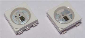
As of now, there are two different revisions of the WS2812 on the market:
The original 6 pin WS2812(S) and the newer 4 pin WS2812B.
The data sheets can be downloaded from the website of world-semi, the original manufacturer, here and here.
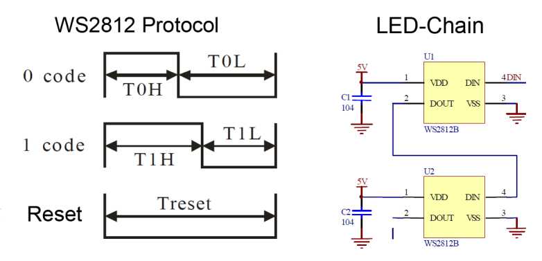
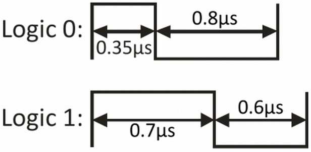
The data transmission protocol itself is relatively simple:
a digital “1” is encoded as a long high-pulse, “0” as a short pulse on “Din”.
When the data line is held low for more than 50µs, the device is reset.
After reset, each device reads the first 24 bit (GRB 8:8:8) of data into an internal buffer.
All consecutive bits after the first 24 are forwarded to the next device
go through internal data reshaping and are then forwarded via “Dout” to the next device.
The internal buffer is written to the PWM controller during the next reset.
So far so good.
This is where things get confusing.
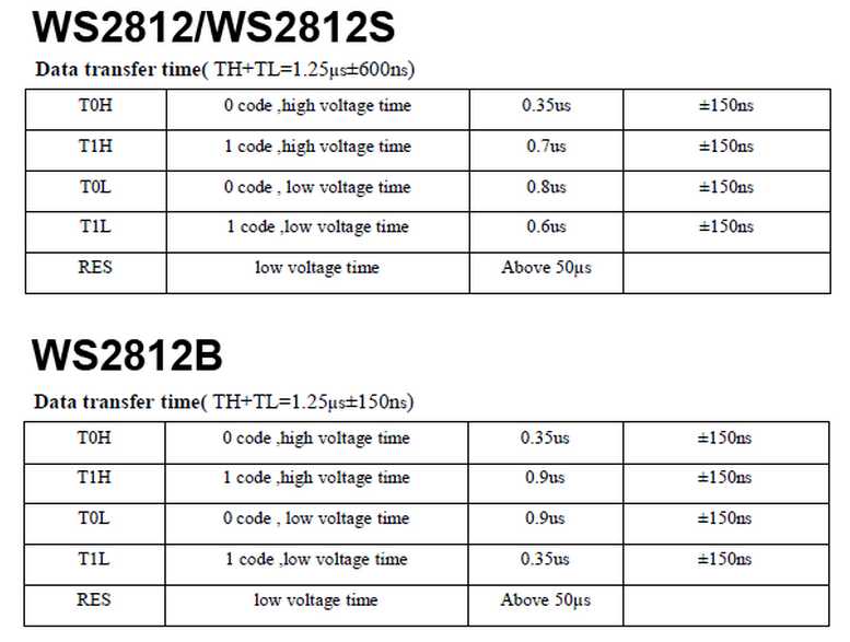
I copied the timing specification from both datasheets above.
As you can see, both devices have slightly different timing for the encoding of the “1”.
Furthermore, the tolerances for the “data transfer time” are completely different and are in conflict with the “voltage time”.
So what are the real tolerances and can we find a set of timing parameters that fits both devices?
Luckily there is a relatively easy way to probe the inner workings of the device:
When data is forwarded, it is passed through the internal reshaping mechanism.
Therefore we can exercise Din and verify the correct interpretation of the input data by comparing it to Dout.
To do this, I hooked a single WS2812 to a ATtiny 85 which took the role of a signal generator.
I then monitored both Din and Dout with a Saleae logic analyzer.
There are some issues with aliasing, since the maximum sampling speed is only 24 Mhz,
but the data seemed still sufficient to understand the WS2812.
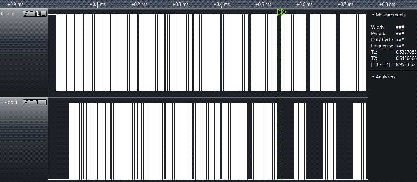
In my first experiment I tried to determine the minimum time needed to reset the LED.
My program emitted blocks of 48 bits with increasing delay time in between the blocks.
As you can see above on the left side, all input data is forwarded to the output if the reset delay is too short.
Once a certain delay threshold is reached, a reset is issues
and data forwarding will only start after the first 24 bits, as seen on the right side.
For the WS2812 under test here, the minimum reset length was 8.95 µs, way below the specifications.
The suggested reset time of 50 µs is therefore more than sufficient to reset the LEDs.
On the other hand, it means that no more than 9 µs of idle time may occur during data transfer,
or a reset may mistakenly be issued.
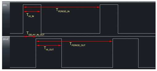
In the next step I looked at the data timing itself.
The image above shows an exemplary measurement of input and reshaped output waveforms.
Both waveforms can be described by two parameters each:
The duration of the hi pulse and the total period.
I programmed the microcontroller to cycle through all possible pulse input combinations
between 62.5 ns (1 CPU cycle at 16 MHz) and 4 µs with a granularity of 62.5 ns.
You can find the code is here.
My original intention was to perform an automatic evaluation of the captured data to create a shmoo plot.
However, I quickly noticed that the behavior was quite regular and instead opted to analyze the data manually.
One of the first observations was that the delay between the leading edge of the input pulse
and the leading edge of the output pulse, T_delay_in_out, was constant regardless of the timing of the input pulse.
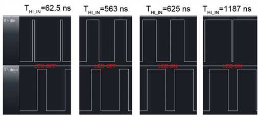
The image above shows a variation of T_hi_in for a constant T_period_in.
The period length, calledtotal data transfer time in the datasheet was set to the specification value of 1250 ns.
As is obvious, there are only two states of the output signal:
A short pulse for a “0” and a long pulse for a “1”.
Even the shortest input pulse (62.5 ns) is identified as “0”, w
hile even the longest input pulse (1250-62.5=1187.5 ns) is identified as a “1”.
The threshold between “0” and “1” is somewhere between 563 and 625 ns.
The LED brightness changes accordingly, suggesting that the observations
from the output signal are indeed consistent with the internal state of the LED.
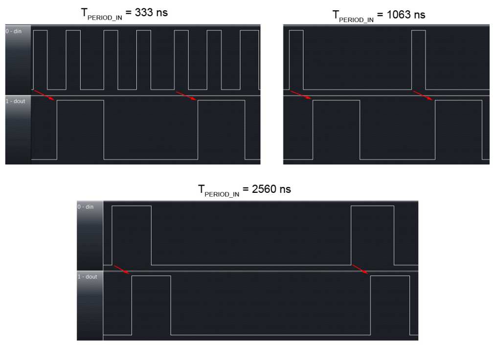
Next, I varied T_period_in.
When the period time of the input signal was much shorter than 1250 ns,
the WS2812 started to reject input pulses.
As can be seen for 333 ns, only about every fifth input pulse is replicated in the output pulses.
The shortest pulse period time where all input pulses appeared on the data output was 1063 ns.
Below that the input pulses were partially or fully rejected.
Above this threshold all input pulses were interpreted correctly
and the period of the output signal reflected the period of the input signal up to 9 µs when the reset condition was met.
This is an interesting observation, because it means that while there is a strict lower limit for the period time of the input signal,
there is no real upper limit. For practical purposes, this allows relaxed timing in the software driver.
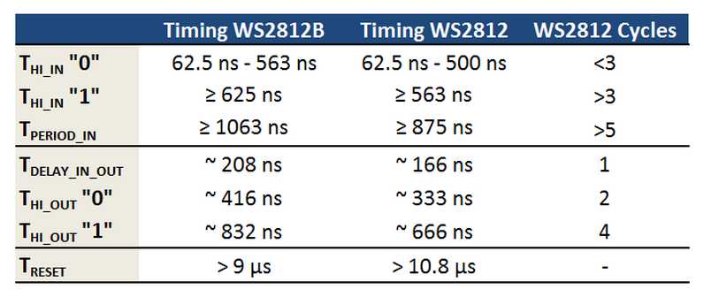
The table above summarizes my findings from the WS2812 and WS2812B each.
It is possible that there are significant differences between production batches of both types,
therefore these number can only serve as a rough indication.
All timings seem to be a bit shorter on the WS2812.
This is consistent with the data-sheet which indicates a longer pulse time for the “1” on the WS2812B.
An interesting observation is that the timing values for both LEDs are multiples of a smaller number,
~208 ns for the WS2812B and ~166 ns of the WS2812.
It appears that the internal controller circuit is actually a clocked design – possibly realized by a small state machine.
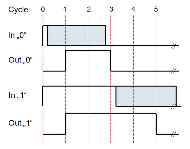
This becomes much more obvious with the diagram above, which normalizes the timing to “WS2812 cycles”.
The internal WS2812 state machine only needs to sample the input twice per bit:
First, it waits for a rising edge of the input.
This will initiate the sequence above.
The input is latched again after cycle 2.
The voltage of the input pin at this point determines whether a ‘1’ or a ‘0’ is read.
Depending on whether the LED already has received 24 bits or not,
this value will either be loaded into an internal shift register or decide whether a 2 or 4 cycle ‘hi’ level signal is emitted.
The sequence ends after cycle 5 and repeats again with the next rising edge.
So, what did we learn from this?
Light_WS2812 library V2.0 – Part II: The Code
After investigating the timing of the WS2812 protocol in the previous part,
the question is now how to use this knowledge for an optimized software implementation of a controller.
An obvious approach would be to use an inner loop that uses a switch statement
to branch into separate functions to emit either a “0” symbol or a “1” symbol.
But as it is often, there is another solution that is both more elegant and more simple.
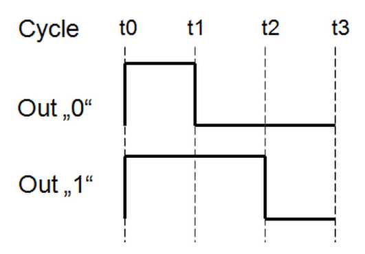
The image above shows the timing of both the “0” and the “1” code.
The cycle starts at t0, the rising edge, for both symbols.
The output has to be set high regardless of the symbol.
At t1, the output has to be set to low for a “0” and can be unchanged for a “1”.
At t2 the output goes low for the “1”. Since it is already low for a “0” we can set the output to low,
regardless of the symbol.
Finally, at t3 the complete symbol has been sent and the output can be left unchanged.
So, in the end there is only one point in time were the output is influenced by the symbol type,
t1.Everything else remains unchanged.
This means that special case handling can be limited to a very small part of the code.
This is what I ended up with in AVR assembler code:
       ldi   %0,8                         Loop 8 times for one byte
loop:
       out   %2,%3     // [01]    - t0    Set output Hi
       ...wait1...
       sbrs  %1,7      // [02/03] -       Skip t1 if bit 7 is set
       out   %2,%4     // [03]    - t1    Set output Low
       ...wait2...
       lsl   %1        // [04]    -       Shift out next bit
       out   %2,%4     // [05]    - t2    Set output Low
       ...wait3...
       dec   %0        // [06]
       brne  loop      // [08]    - t3    Loop
This code outputs one byte of data, which has to be loaded into %1 (The C compiler will take care of this).
Since the protocol sends data msb first, bit 7 is tested. If it is “1”, the out instruction at t1 is skipped.
That’s it, as simple as that, only 7 instructions needed in the inner loop.
What is left now is to correct the timing. To do that, nops have to be inserted at positionswait1..wait3.
As shown in the previous part, the most critical timing is that of the “0”
where the delay between t0 and t1 may not exceed 500 ns.
The minimum achievable delay, when no nops are inserted at wait1, is two cycles.
This equals 500 ns at 4 MHz and less at higher clock speeds.
All other timings may exceed the minimum timing required from the data sheet.
This means that even this simple loop is able to control WS2812 LEDs at only 4 MHz!
This is quite an achievement, since it was previously considered to be difficult to control WS2812 LEDs even at 8 MHz.
Note that the 500 ns is safe on the WS2812B, but may be critical on the WS2812(S). It worked with my devices, though.
To make the final implementation as flexible as possible, I
opted to calculate the exact number of nops to insert at compile time from the F_CPU define,
which is usually set to the CPU clock speed in the AVR-GCC toolchain.
You can find the implementation here. The C-code tries to adjust the timing according to the following rules,
which considers at least 150 ns margin for both the WS2812 and the WS2812B timing:
 350 ns <  t1-t0 <= 500 ns
 900 ns <= t2-t0
1250 ns <= t3-t0
The outer loop is implemented in pure C, since it can be safely assumed not to take more than 5 µs. This way maximum flexibility is retained.
OctoWS2811 is a high performance WS2811 & WS2812 & WS2812B LED library,
written by Paul Stoffregen, featuring simultaneous update to 8 LED strips
using efficient DMA-based data transfer (technical details below).
Minimal CPU impact and double buffering allows complex animation.
A VideoDisplay example is included, capable of scaling to extremely large LED installations
using multiple Teensy 3.0 or 3.1 boards with a frame sync signal for precise refresh timing.
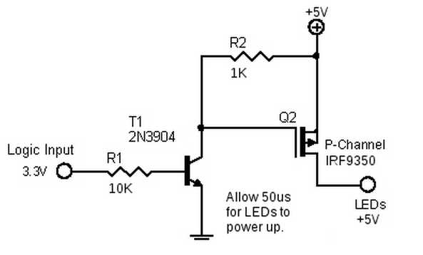
When the LED is off, the WS2811 chip consumes approximately 0.9 mA of current.
For battery powered LEDs, this current can easily drain the battery.
A P-channel MOSFET transistor or similar switch may be needed to disconnect power from the LEDs,
if the battery remains connected when the LEDs are not in use.
This circuit was recommended by David Beaudry to manage the power.
David also tested Vishay SUP75P03-07-E3 and SI4465ADY-T1-E3 transistors, which are able to power more LEDs.
OctoWS2811 is designed for highly efficient data output to WS2811-based LEDs,
able scale to very large LED arrays.
The WS2811 requires very specific waveform timing. Each LED uses 24 bits,
each 1.25 µs, for a total of 30 µs per LED in the strip.

Driving 8 LED strips simultaneously allows each strip to be only 1/8th the length.
All LEDs update 8X faster than driving only a single long strip.
1000 LEDs can be updated in 3.8 ms, which allows a theoretical update rate of 240 Hz.
The VideoDisplay example implements a Frame Sync signal,
allowing many Teensy 3.0 boards to work together, each driving 1000 LEDs.
The boards precisely synchronize their update, even if the USB delivers data to the many boards with some varying latency.
Fast update times are preserved when scaling up to extremely large LED arrays.
OctoWS2811 uses Direct Memory Access (DMA) to create the WS2811 waveforms with nearly zero CPU usage.
Because the CPU is free and interrupts remain enabled, the processor is free to receive data
or perform computations in preparation for the next frame of display,
while the previous one is still be transferred to the LEDs.
The 8X faster update and free CPU time the key differences between OctoWS2811 and other libraries,
which create the WS2811 waveforms for a single strip using carefully timed software.
DMA is a special hardware feature which allows data to be automatically
moved between memory and I/O registers in response to hardware events,
without any CPU usage (other than initially configuring parameters).
OctoWS2811 uses 3 DMA channels to synthesize the WS2811 waveforms.
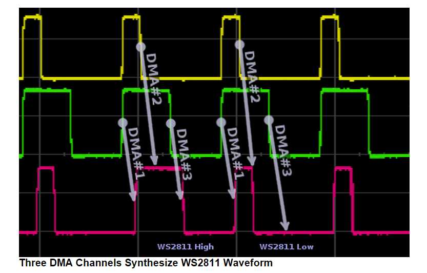
The hardware events which trigger the DMA channels are a pair of PWM waveforms,
corresponding to the WS2811 bit low and high waveforms.
The rising edge (both PWM rise at the same moment) triggers channel #1,
which copies a fixed byte (0xFF) to an I/O register which sets all 8 output bits,
causing the WS2811 waveform to begin each bit.
The first falling edge triggers DMA channel #2, which copies one byte of the actual frame buffer data to all 8 pins.
The bits which are low transition to low at the correct time to create a zero bit to each WS2811 LED.
The bits that are high have no effect, because channel #1 already set all 8 pins high.
The 3rd DMA channel triggers at the second falling PWM edge, causing all the WS2811 bits to be written to zeros.
The pins which were left high by channel #2, become low, as required by the WS2811 timing for a one bit.
The pins which were already low are not changed.
Together, these 3 I/O updates create a WS2811 waveform automatically without any CPU activity.
The ARM-based chip from Freescale used on Teensy 3.0 has crossbar switch and dual-bus RAM,
which allows the DMA and ARM CPU to work together very efficiently.
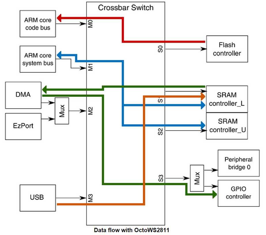
0xWS2812 STM32 driver for WS2812(B) RGB LEDs
标签:
原文地址:http://www.cnblogs.com/shangdawei/p/4762035.html