标签:
Wireless charging of portable electronic devices is here now. It will become ubiquitous when all such devices adhere to the same standard.
The Wireless Power Consortium (WPC) has developed a standard for wireless power systems referred to as Qi (pronounced as “chee”). This Qi-compliant wireless power system allows compatibility between devices from multiple manufacturers. It also allows handheld equipment from original equipment manufacturers (OEMs) to focus exclusively on the design of their equipment without having to design a customized wireless power pad, since multiple Qi-compliant power sources are already available.
The key to interoperability within the Qi standard is the communication protocol. This article explains the fundamentals of how the receiver (RX) device (handheld equipment) communicates with the transmitter (TX) device (charging pad providing energy). Communication packets sent by the receiver (and the corresponding response from the transmitter) are illustrated. Communication from the receiver to the transmitter allows the closed-loop control and regulation of the receiver circuit’s output voltage.
Introduction
Wireless power systems are emerging as a practical option for conveniently recharging mobile phones and other handheld devices. Implementing an industry standard interface allows a common charging pad (TX) to recharge multiple types of battery-operated devices (RX). The WPC developed the Qi standard for wireless power systems with up to 5W of output power. This allows complete interoperability between transmitters and receivers independent of device manufacturer.
This standard defines the means of implementing a number of functions that enhance the utility and efficiency of a wireless power system, for example:
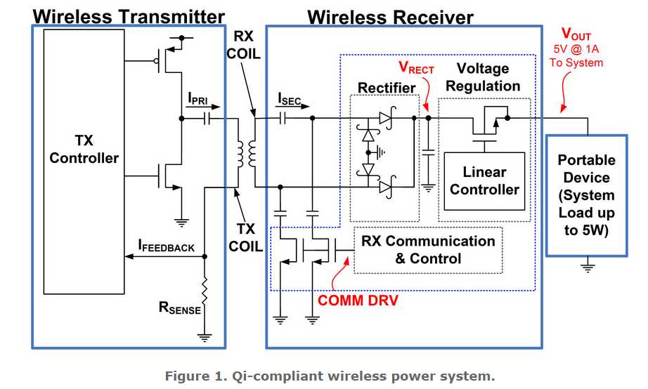
Figure 1 shows a block diagram of the overall Qi-compliant wireless power system.
References 1 and 3 provide a more complete description of the wireless power system.
Basics of Communication
The resonant converter in the TX circuit generates a quasi-sinusoidal AC signal in the range of approximately between100-200 KHz across the primary TX coil. This signal is magnetically coupled into the secondary RX coil, where additional circuitry rectifies and regulates it to provide DC output to the handheld device.
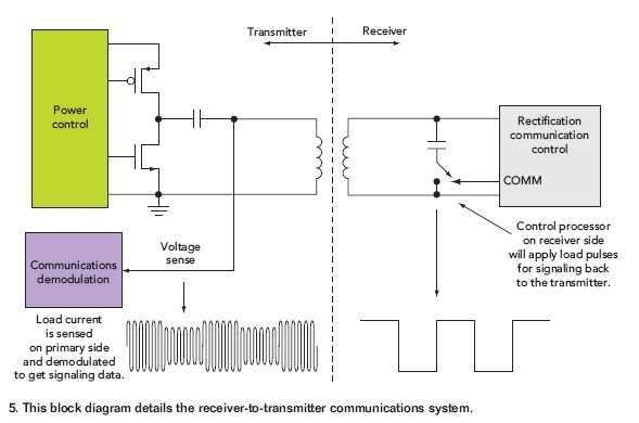
Communication from the RX back to the TX uses the same magnetic coupling path as the forward power transfer. A simple load modulation method is used to communicate status and commands back to the TX controller. When the receiver circuit is powered-up, it can apply a controlled pulsed load across the secondary coil (Figure 2). This results in an amplitude modulation of the primary coil voltage which is detected and demodulated by the TX controller.
The load modulation can use either a resistive or capacitive load element. The modulated load is internal to the RX side circuitry and independent of the actual system load (battery or portable device).
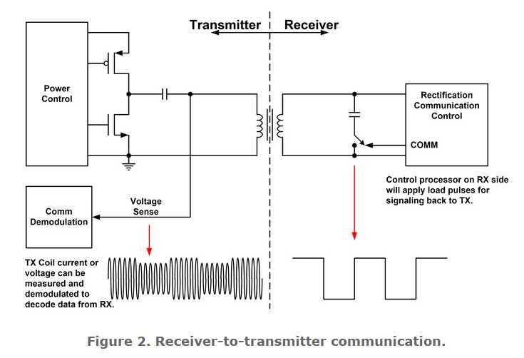
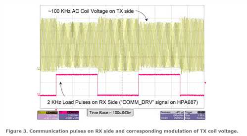
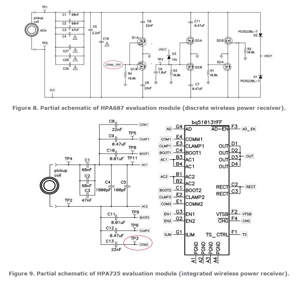
Figure 3 shows an example of the actual effect seen on the primary TX coil voltage as a result of the modulation pulses on the secondary RX side. These waveforms correspond to the ideal waveforms illustrated in Figure 2. The modulating signal on the RX side is measured at the point labeled “COMM DRV” in Figure 1.
Communication packets
The data in Figure 3 shows that load pulses on the RX side correspond to an amplitude modulation effect on the primary side (TX coil voltage and/or current). The communication from the RX side uses a “differential bi-phase” bit encoding scheme. Since there is no separate clock line or control signal path, a fixed clock frequency of approximately 2 Khz is used with a start bit before each 8-bit transmission, followed by parity and stop bits. Figure 4 illustrates the bit / byte encoding schemes as defined in the WPC Specification v1.0.2 (Reference 1).
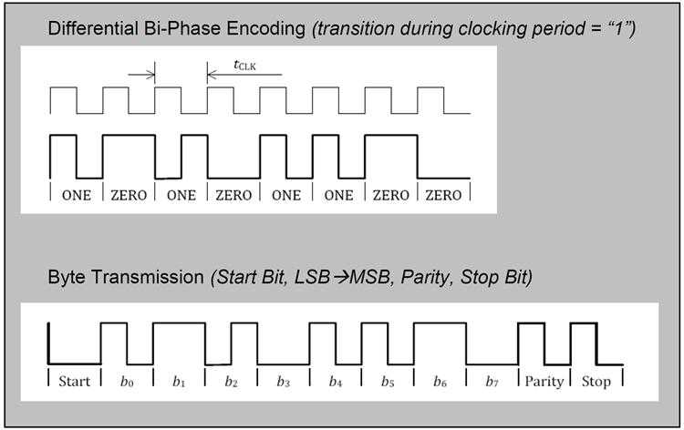
A communications packet consists of four specific sections:
A number of specific functions are defined by the types of packets that can be sent. As of now, not all possible options are implemented, but room is still available for expansion of functionality with future versions of the Qi standard. Reference 1 provides a complete description of existing packet types. The most common packets and their functions are:
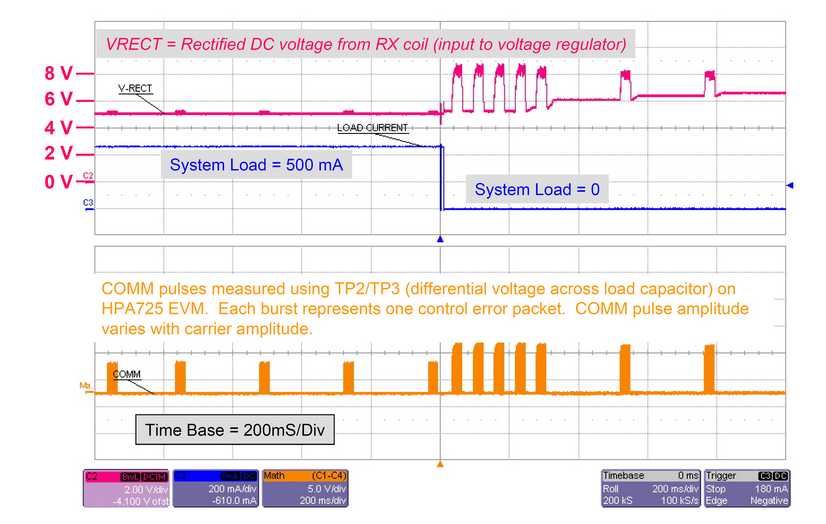
Figure 5. Control error packet transmission and VRECT voltage response to a negative load transient (500 mA to 0 mA).
Optimizing load transient response using RX-to-TX communication
The ability of the RX side circuitry to communicate back to the TX side circuitry allows the overall wireless power system to act as a true closed-loop regulated power system, since the equivalent function of an analog error signal feedback is accomplished by the RX controller‘s control error packets being sent back to the TX controller. From an overall system point of view, the implementation shown for the wireless power TX/RX combination can be treated as a switch-mode converter with a low-dropout (LDO) post-regulator.
The raw input voltage to the RX coil can be highly variable in an "open loop" configuration as it will fluctuate significantly with variable load. To maintain good regulation of the final DC output (for example, +5V), the feedback provided from the RX side adjusts the input to the linear regulator (VRECT) up or down, based on the load current conditions.
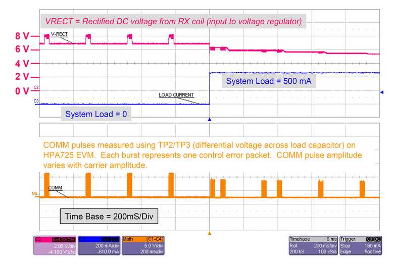
Figure 6. Control error packet transmission and VRECT voltage response to positive load transient (0 mA to 500 mA).
When the output is lightly loaded, the RX circuit sends control error packets back to the TX controller to increase the VRECT input voltage applied to the LDO stage up to approximately +7V. The regulated output is set to +5V. Since the load current is light, the 2V input-output differential across the LDO does not represent significant power loss.
The reason for setting the VRECT level higher at light loads is to anticipate the effect of a low-to-high current transient. When this transient occurs, the VRECT voltage initially sags until the RX controller can respond. The error packets sent by the RX controller request the TX controller to raise the output voltage. Leaving the VRECT level high at light loads provides enough headroom to prevent the +5V regulated output from collapsing until the digital communication (feedback) can be sent.
At higher load currents, the VRECT voltage is kept as low as possible to minimize power loss across the LDO (and maximize total system efficiency). For example, at the maximum load current of 1.0A, the VRECT signal is set to approximately 5.20V. For example, the dropout performance of the LDO regulator stage within the bq51013 (wireless receiver IC) allows it to maintain a regulated 5.0V at 1.0A load current.
Figures 5 and 6 illustrate the adjustment in the VRECT setpoint based on load current described earlier. Note that the COMM signal bursts shown correspond to complete packets rather than individual bits due to the time scales of the plot. When the VREC deviates significantly from the desired setpoint by a large error, the COMM packets are sent at a faster interval. As the VRECT approaches the desired setpoint, the COMM packet transmission interval is decreased.
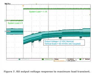
Figure 7 shows the system output voltage response to a large load transient (corresponding to the maximum load transient case of 0A à 1A). The maximum load transient results in less than 100 mV droop at the output, such as an approximate two percent deviation from the regulated output voltage.
Measurement of RX and TX signals
Qi-standard wireless power devices allow a system designer to implement a Qi-compliant power system using an integrated solution, such as the bqTESLA™, and requires no programming implement the communications protocol. Evaluation modules (EVMs) are available for both TX controller and RX controller sections.
Figures 8 and 9 are partial schematics from the bqTESLATM evaluation modules which highlight the measurement points used to collect the data in Figures 3, 5, 6, and 7. In the case of the discrete receiver circuit (>SLVU420), the COMM DRV signal can be directly measured since the load modulation FETs are external to the RX controller IC. When using the integrated RX circuit (SLVU477) the load modulation FETs are integrated within the RX controller and their gate drive signals cannot be accessed. However, the communication pulses from the RX controller still can be detected by measuring the differential voltage across the load capacitor C13 as shown. The complete schematics of the bqTESLATM EVM kits are provided in Reference 4 and 5.
Summary
When using a fully integrated Qi-standard chipset solution, all of the communication from receiver to transmitter is handled automatically with no user programming required. However, a basic understanding of the communication protocol can help the system designer know how to test and verify that the system is operating properly.
At a fundamental level, the communication can be thought of as amplitude modulation (AM) with a modulation frequency of 2 KHz and carrier frequency ranging from 100 to 200 KHz. This simple, robust protocol defined by the WPC Qi standard allows communication to occur along the same inductively coupled path as the forward power transfer, and does not require a separate set of contacts or magnetics.
The wireless power receiver’s ability to communicate its power needs back to the transmitter (based on load conditions) allows the system to maintain a stable output voltage under constant or transient load conditions. The closed-loop nature of the overall system is achieved by using a Qi communication protocol.
Acknowledgements
The authors would like to thank Steve Terry, Tony Antonacci, and Michael Day for their technical and editorial contributions to this article.
References
Communication within the WPC is from the receiver to the transmitter, where the receiver tells the transmitter to send power and how much.
In order to regulate, the receiver must communicate with the transmitter whether to increase or decrease frequency.
The receiver monitors the rectifier output and using Amplitude Modulation (AM), sends packets of information to the transmitter.
A packet is comprised of a preamble, a header, the actual message and a checksum, as defined by the WPC standard.
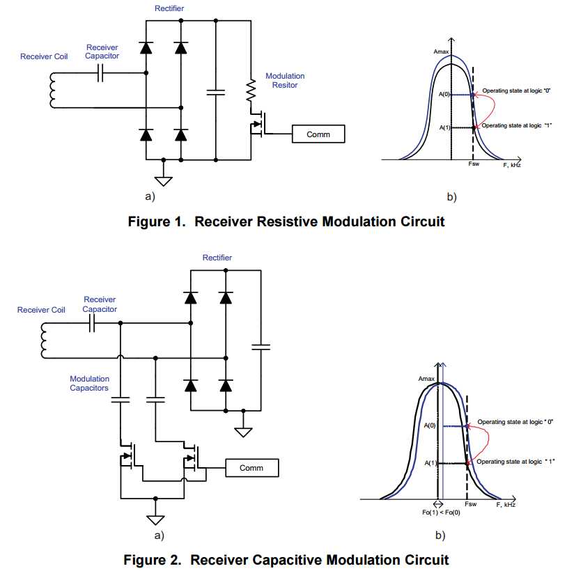
The receiver sends a packet by modulating an impedance network.
This AM signal reflects back as a change in the voltage amplitude on the transmitter coil.
The signal is demodulated and decoded by the transmitter-side electronics and the frequency of its coil-drive output is adjusted to close the regulation loop.
The bq500410A features internal digital demodulation circuitry.
The modulated impedance network on the receiver can either be resistive or capacitive.
Figure 1 shows the resistive modulation approach, where a resistor is periodically added to the load,
Figure 2 shows the resulting amplitude change in the transmitter voltage.
Figure 2 shows the capacitive modulation approach, where a capacitor is periodically added to the load and the resulting amplitude change in the transmitter voltage.
RT1650是全集成的无线电源接收器,可为移动设备提供7.5W的电源供应。本文解释了无线电源传输的基本原理,简要介绍了各种无线电源传输的标准,重点介绍了名为Qi的WPC 1.1低功率标准的实现方法,对RT1650的主要特性进行了讲解。文章最后以Nokia DT601无线电源发射器和以RT1650为核心的EVB结合在一起所构成的无线电源传输系统为例对实际应用中可能遇到的各种问题进行了讲解,具有重要的参考价值。
在两个装置之间,无实体缆线连接而能传输电源之方式有许多优点:
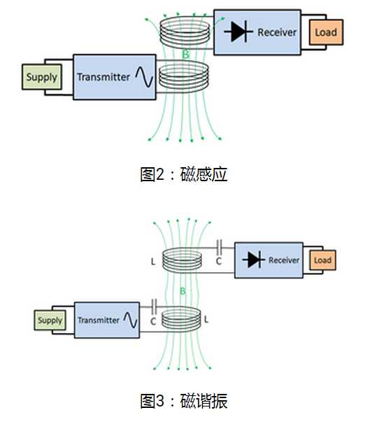
最常见之无线电能传输方法是透过两个耦合的电感器之间的磁感应来实现的,交流变压器即为应用此原理之一例,线圈附近的磁场强度是随距离呈指数关系下降的,换言之,若要高效率的电源传输,就必须使发射器线圈和接收器线圈之间的距离尽可能地近,或是其距离要远小于线圈的直径,以达到高效率的电源传输。
另一种允许发射器和接收器线圈之间的距离较大的方法称为谐振感应耦合法,。在这种系统中,发射器和接收器的内部都有谐振在相同频率上的LC电路,电源就在这一谐振频率上被传输。两个线圈之间的谐振可加强相互之间的耦合,并改善电源传输的效率。此方式允许的发射器和接收器线圈之间的距离可较大,但和磁感应式相比,其最大可传输功率较低。
随着需要定期充电的便携设备(如手机,平板计算机和笔记本计算机)的用量的增加,无线电源联盟(Wireless Power Consortium ,WPC)于2008年成立,其使命为制定在电子装置之间进行无线电源传输的标准。 2009年,WPC 推出了命名为Qi 的低功率标准,使得任何符合 Qi 标准的装置之间能够以磁感应方式传输5W以下的电源。
目前,针对无线电源传输的标准有三种:Qi,PMA和A4WP。Qi和PMA 都是应用磁感应原理,而A4WP则是采用谐振感应原理。表一显示了这三种标准之间的差异。
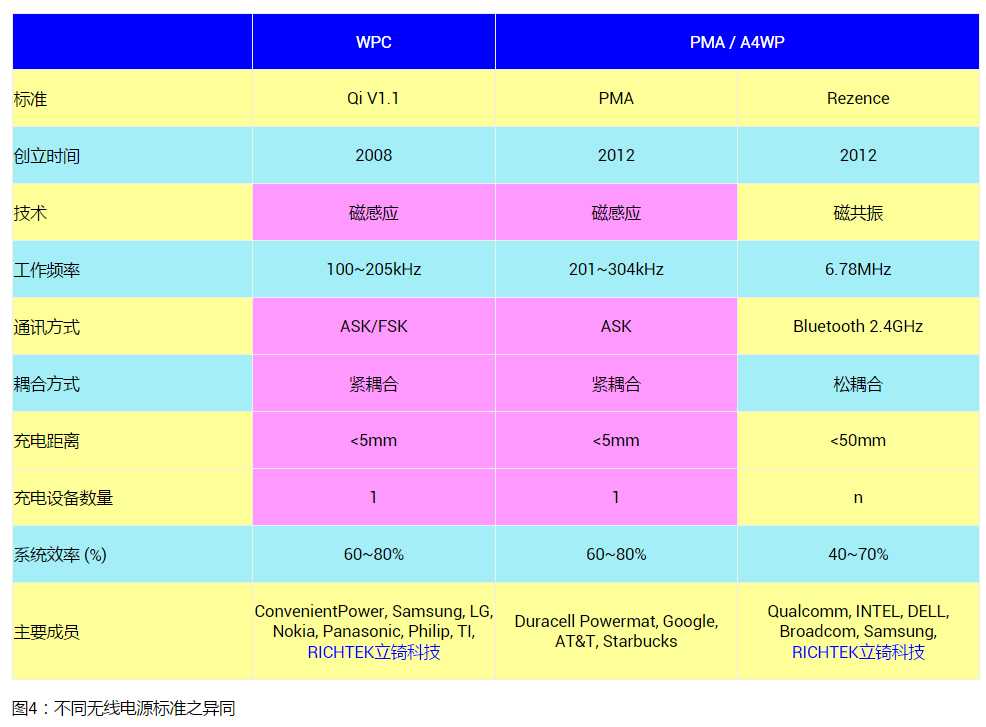
Qi 和PMA标准的性能非常接近,容许电源传输在短距离(通常约为5毫米)上对单一接收装置进行,发射器和接收器之线圈必须对齐以实现高效率的电源传输,两装置之间的通讯透过所传输的电源信号进行,避免了额外硬件的使用。Qi和PMA在通讯协议上是有差异的。
Rezence(先前的称呼是A4WP)使用磁谐振感应耦合技术, 允许在较大的距离下 (高达约50毫米) 传输电源,发射器和接收器之线圈不需要很好地对齐,其缺点是全系统效率较低,能传输的功率较低。接收器和发射器之间以蓝牙作为通讯手段,这使多个设备之间的通讯成为可能,因此容许多个装置从一个发射器接收电源。由于需要额外的硬件实现蓝牙连接,此解决方案的成本较高。
Qi WPC 1.1*低功率标准(5W)是目前被最广泛采用的手机无线供电方法。
*新的WPC 1.2标准已于2015年6月发布,RT1650接收器可以兼容WPC 1.1和WPC 1.2。
WPC 1.1标准中,接收器对发射器的通信采用ASK(幅度键控)的反向散射方法进行:接收器通过对接收到的来自发射器的信号的幅度进行调制,该信号幅度的变化会被反射到发射器一侧,再经解调、解码以后供系统使用。
在我们的案例中,接收器一侧的ASK调制由开关控制的与接收到的交流信号并联的电容来实现,这相当于给交流信号增加了一个额外的负载,它将导致交流信号电压的下降(或者说是增加了交流信号的电流)。这种被改变了的交流信号幅度会被反射到发射器一侧,发射器可以检测到交流信号的变化,这种变化可在信号电压或电流的包络上看出来,经过对它的解调制操作以后即可取得其原始信息。
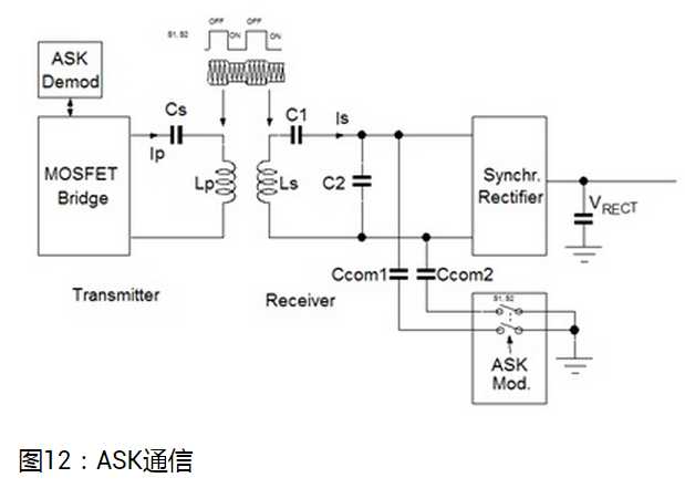
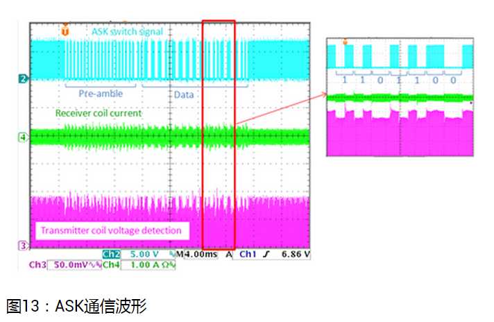
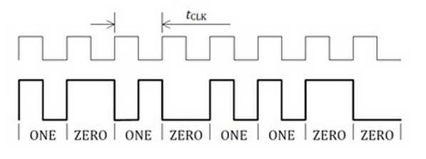
通过图13的波形可以看出ASK调制的基本表现形式。由于是串行信号,它包含了时钟信息和数据,其第一部分是前置的用于时钟同步的信号,紧接着是数据包的头部、被编码的信息,最后是校验码。信息的传输采用了差分双相编码方式,如下图所示
无线电源传输 Wireless Power Consortium (WPC) Communication
标签:
原文地址:http://www.cnblogs.com/shangdawei/p/4882351.html