标签:
What amplifiers are used to drive analog-to-digital converters (ADCs)?
Possibilities include single-ended and differential inputs and outputs,
plus voltage feedback (VFB) or current feedback (CFB) in the control loop.
Specialized amplifiers may provide level shifting, interstage isolation, single-ended to differential conversion,
differential to single-ended conversion, plus attenuation or gain.
What are the considerations with VFB and CFB amplifiers?
With CFBs, closed-loop gain is largely independent of frequency.
Also, CFB amps provide faster slew rate and lower distortion and perform well at higher gains than VFB amps.
VFBs can offer lower noise and better dc performance than CFB amps.
Other tradeoffs lie in design constraints. With a VFB op amp, the circuit designer
has considerable freedom in choosing the value of the feedback resistor, although higher resistance values may limit stability.
CFB amplifier datasheets specify the feedback resistor values.
CFBs therefore lend themselves to applications that require higher gain levels.
What are the advantages of differential ADC drivers?
These drivers facilitate singleended-to-differential and differential-to-differential conversions,
common-mode level shifting, and amplification of differential signals.
They also exhibit lower distortion and faster settling time than singleended drivers.
How can a differential VFB ADC driver differ from a single-ended amplifier?
In addition to the usual inverting and non-inverting inputs, some differential VFB ADC drivers have another input,
VOCM, that shifts the commonmode voltage of the differential output (Fig. 1)
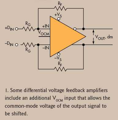
Like a VFB op amp, closed-loop gain is set by means of input and feedback resistances, but there must be separate,
matched resistors for the inverting and non-inverting inputs.
The internal common-mode feedback loop produces outputs that are highly balanced
over a wide frequency range without requiring tightly matched external components.
Thus, differential outputs are very close to the ideal of being identical in amplitude and are exactly 180° out of phase.
Also, if it is necessary, preserving the dc content of a signal can be accomplished via the VOCM function.
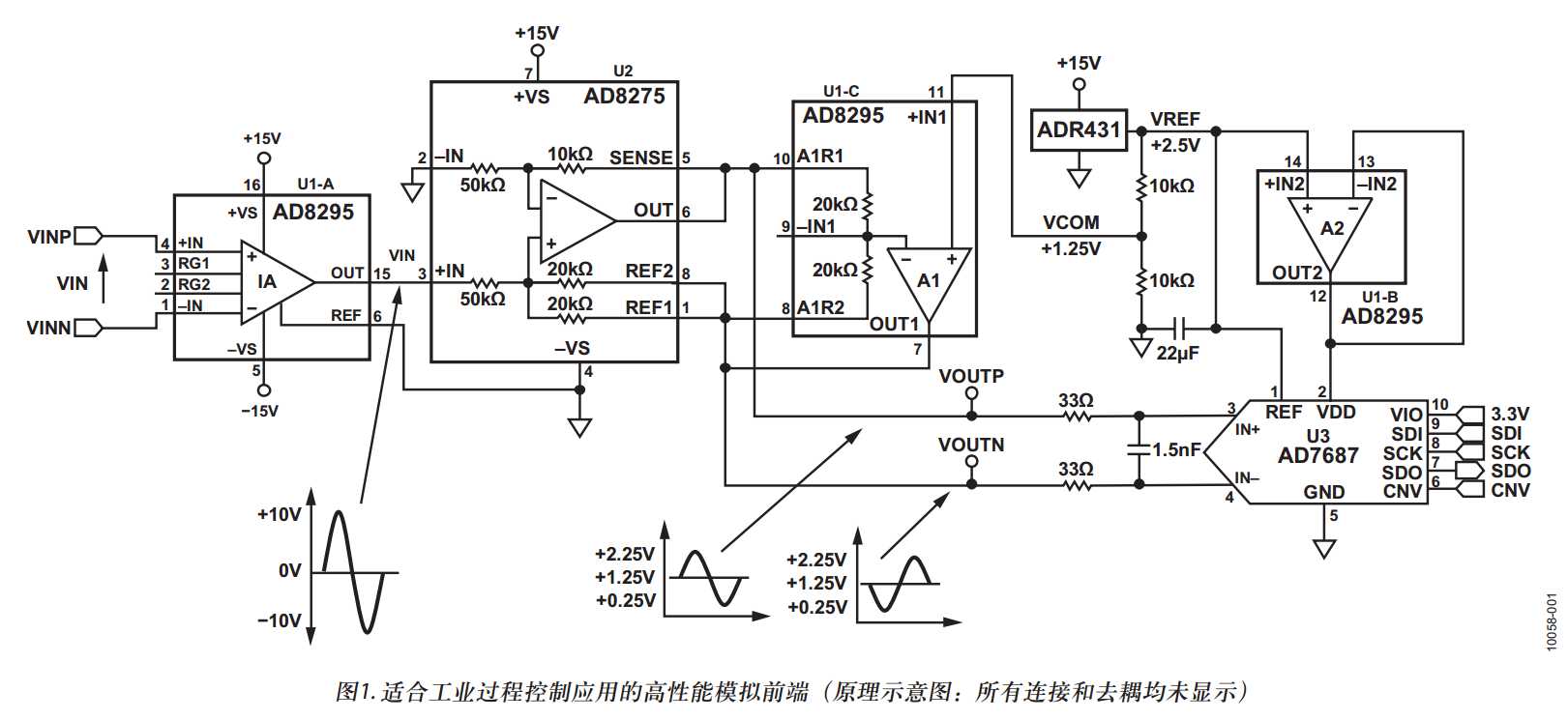
When would I need a single-ended, attenuating, level-translating ADC driver? How does it work?
Industrial applications often involve sensors driven by ±10-V signals.
That’s a problem with single-ended input ADCs fabricated to today’s smaller design rules because those ADCs are constrained to a smaller input signal swing.
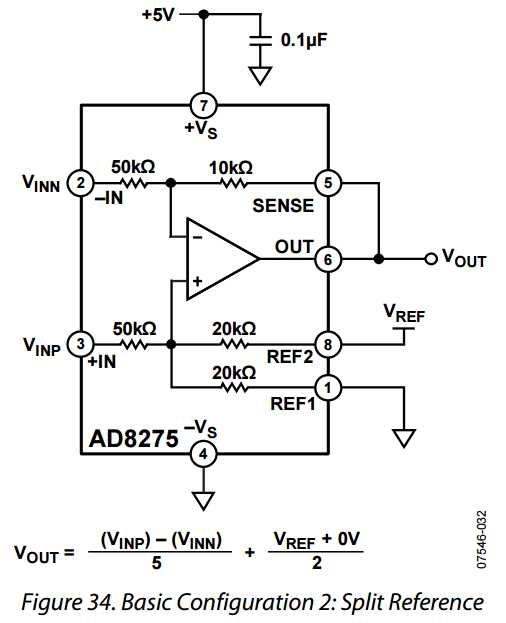
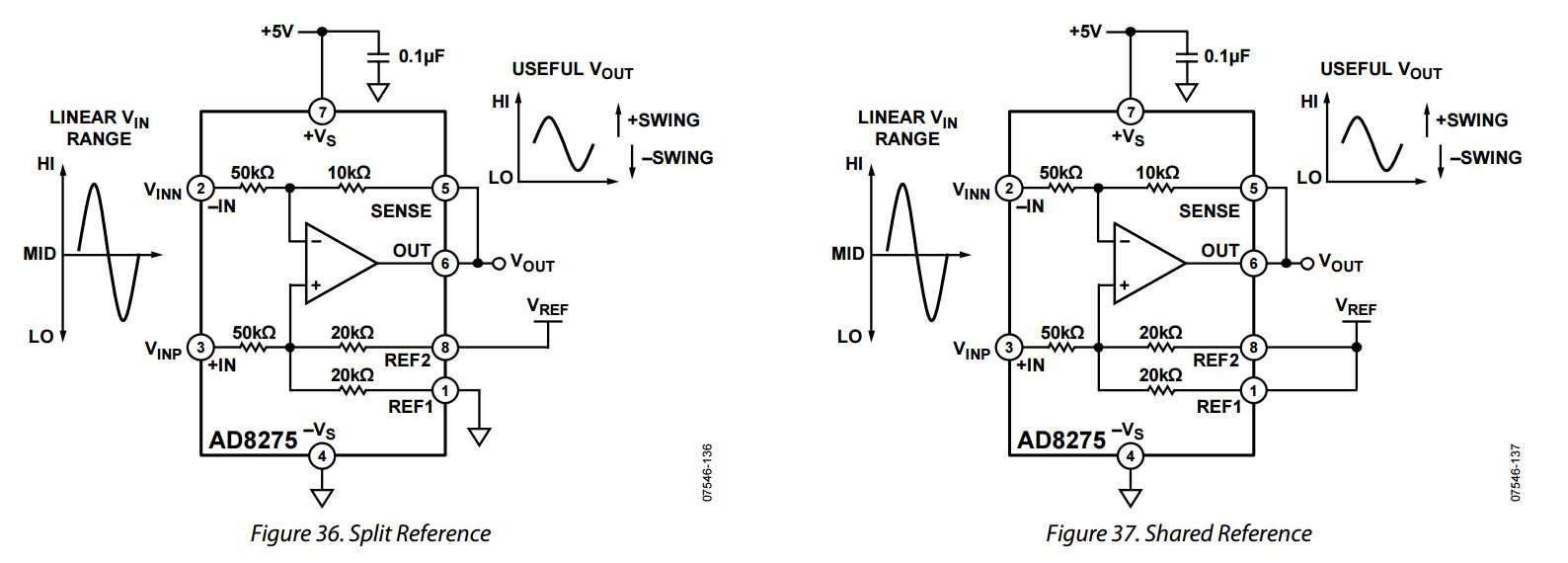
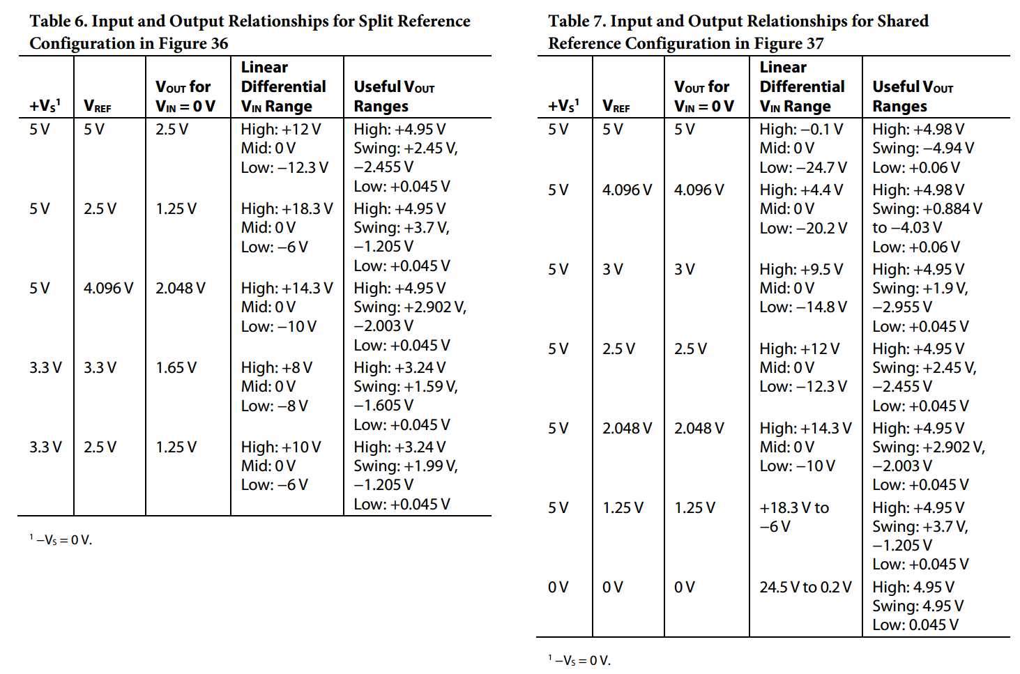
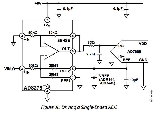
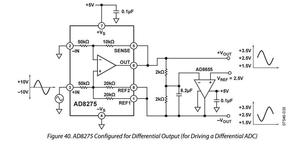
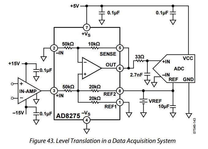
A level-translating ADC driver takes a large signal, reduces the amplitude, and level-shifts the output commonmode voltage
so it is compatible with low-voltage, single-supply ADCs (Fig. 2).
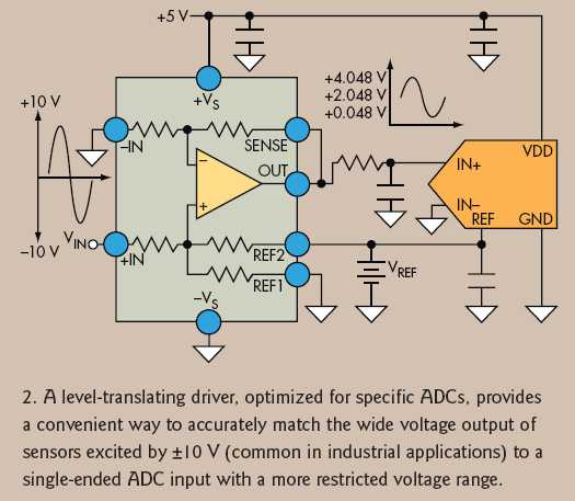
For example, a 20-V p-p (±10-V) input signal riding on 0 V might be converted to a 4-V p-p signal riding on 2.5 V.
There are a number of other ways to perform level-translation.
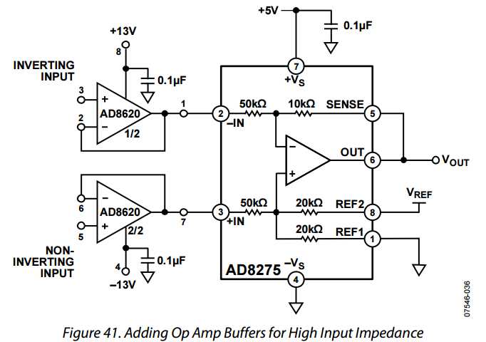
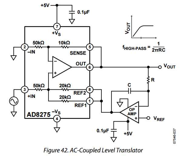
It has been accomplished using multiple amplifiers, single differential drivers like those described above, or ADC drivers designed for level translation.
The approach using a single differential driver is simpler than the multi-amplifier approach, and the specialfunction level translation driver approach is simpler yet.
Such amps use internally lasertrimmed resistors, ensuring high gain accuracy, along with high common-mode rejection and low offset.
A final advantage is that, since the amp and ADC use the same supply voltage as the ADC, there is no need for multiple power supplies.
If a driver has a 1-GHz, –3-dB bandwidth, can I use it at that frequency to drive converter inputs?
If you’re driving a high-resolution ADC, look beyond the –3-dB spec and consider gain flatness and,
in particular, harmonic distortion as a function of frequency.
Recall that in a VFB amp, the –3-dB bandwidth figure simply reflects the half-power point after the amp’s open-loop gain starts its –6-dB/ octave roll-off.
That provides a rough figure for comparing amplifiers.
Your concern as a mixed-signal circuit designer must be to minimize the effect of amplifier distortion on the ADC’s effective number of bits (ENOB) performance.
ENOB is a function of signal-to-noise ratio (SNR) + distortion (SINAD) across the whole analog signal chain:
ENOB = (SINAD – 1.76)/6.02.
So, look to the data sheet graphs of harmonic distortion to make your decision.
Why would I want to use an active driver instead of a passive transformer?
The main reasons are to get better pass-band flatness and to isolate the signal from the noisy ADC input.
Transformers have a rather “lumpy” frequency response.
An amplifier should produce less variability, typically ±0.1 dB over the frequency range.
If the design calls for wideband gain, an amplifier provides a better match than a transformer to the ADC’s inputs.
Still looking at frequency response, some amplifiers provide dc coupling.
Transformers can’t deal with slowly varying signals.
Because transformers are passive devices and provide no interstage isolation,
noise generated on the secondary coil of the transformer from the ADC input will pass through it back to the original signal source.
In contrast, amplifiers buffer the signal source with a low output impedance,
providing 70 to 80 dB of interstage isolation from the ADC input back to the original signal source.
On the other hand, a consideration that favors transformers is that at higher frequencies,
they may maintain better SNR and spurious-free dynamic range (SFDR).
Nevertheless, within the first or second Nyquist zone, a transformer or an amplifier can be used.
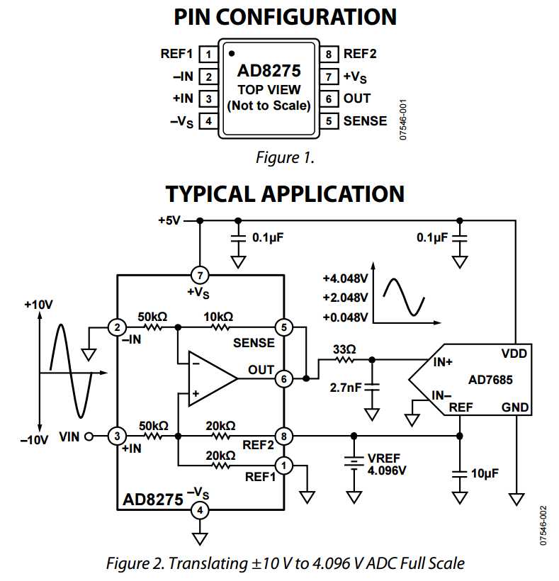
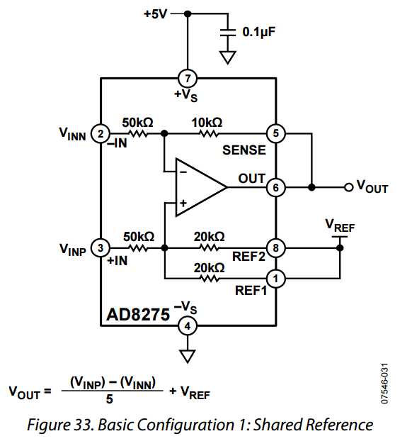
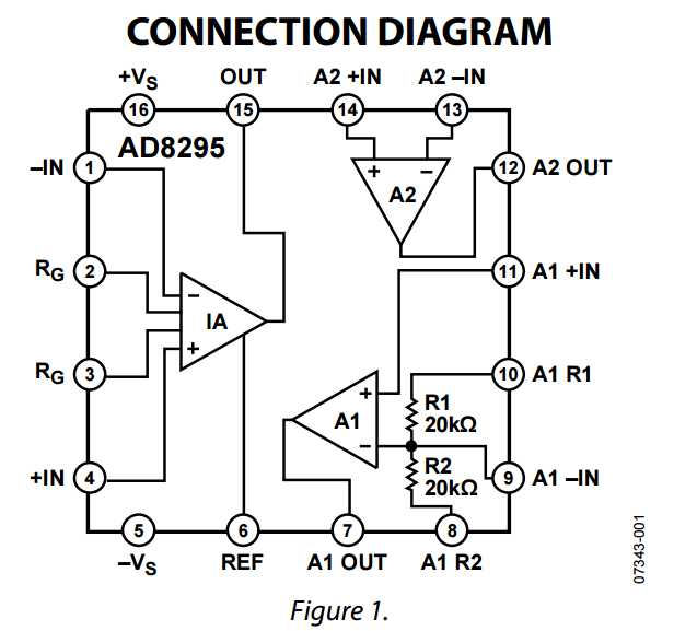
AD8275 Driver Amplifiers For Analog-To-Digital Converters
标签:
原文地址:http://www.cnblogs.com/shangdawei/p/4893539.html