标签:
The process of moving data in and out of the Memory Array and over the Memory Bus is not overly complicated, although the massive parallelization of the actual effort can make it somewhat difficult to fully envision what‘s really happening without some pretty concise visual aids. We‘ll try our best to help you out in this regard.
Both read and write access to DDR[3] SDRAM is burst oriented; access starts at a selected location and continues in a pre-programmed sequence for a Burst Length (BL) of 8-bits, or 1 byte, per bank. This begins with the registration of an ACT command and is followed by one or more READ or WRI commands.
Chip Select (S0#, S1#), one for each rank, either enables (LOW) or disables (HIGH) the command decoder which works like a mask to ensure commands are acted upon by the desired rank only.
The length of the each Read Burst (tBurst) is always 4 clocks (4T) as DDR memory transmits data at twice the host clock rate (4 clocks x 2 transactions/clock = 8 transactions or 8 bits per bank).
The address bits registered coincident with the ACT command are used to select the bank and page (row) to be accessed. For our hypothetical 2GB DIMM described on Page 2 of this article, Bank Selects BA0-BA2 indicate the bank and Address Input Selects A0-A13 indicate the page. Three bits are needed to uniquely address all eight banks; likewise 14 bits are needed to address all 16,384 (214) pages.
The address bits registered coincident with the READ or WRI command are used to select the targeted starting column for the burst. A0-A09 select the column starting address (210 = 1,024). A12 is also sampled during this operation to determine if a Burst Chop (BC) of 4-bits has been commanded (A12 HIGH). Even though a Burst Chop delivers only half that data of a regular Read Burst, the time period to complete the transfer is still the same: 4T. The SDRAM core simply masks the outgoing data clock strobe for the second half of the full read cycle.
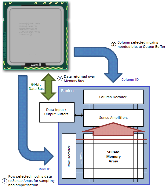
Figure 3. Memory read and write operations can be broken down into a series of well defined events
During a Precharge command A10 is sampled to determine whether the precharge is intended for one bank (A10 LOW; BA selects) or all banks (A10 HIGH).
Data Input/Output pins DQ0-DQ63 provide the 64-bit wide data interface between the memory controller embedded in the CPU and each DIMM. Those with a triple-channel capable CPU, like the Intel Core i7-series processor, will come to understand why the memory bus width is reported as 192-bit – three independently operated channels each with a 64-bit interface makes 192. Those of you running a Core 2 or a Core i3/i5 will have to make do with just two channels for a total bus width of 128 bits.
Each channel can be populated with up to two DIMMs. This means there could be a maximum of four ranks per channel, assuming we install a matched pair of dual-rank modules. Installing more than one DIMM per channel does not double the Memory Bus bandwidth, as modules co-located in the same channel must compete for access to a shared 64-bit sub-bus; however, adding more modules does have the added benefit of doubling the number of pages that may be open concurrently (twice the ranks for twice the fun!).
Figure 3 attempts to provide a top-down look at the minimum cycle needed to first open a page in memory, and then read data from the activated page; Figure 4 shows the same, only from a much more fundamental perspective; and Figure 5 provides a detailed accounting of the timing involved.
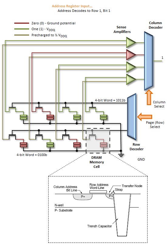
Figure 4. Now it all makes sense! (pun intended)
In this example we assume the bank has no open page, thus is already in the proper precharged state to support a new page access command. Step 1 selects the bank; Step 2 selects the column; and Step 3 bursts the data out over the Memory Bus. A 1-bit row address and a 2-bit column address are all we need to read any data stored in our 2 x 4-bit x 1 (bank) Memory Array.
An Activate command prompts the routing of the specified page address to be accessed to the Row Decoder where it triggers the chosen Word Line to appear at the input of the Sense Amps. As previously stated, this takes a finite time - Row-Column (or Command) Delay (tRCD) is used to program the minimum wait time the memory controller allows for this to occur before it issues the next command in the sequence. Attempting to set too low a timing can lead to inconclusive operation, often resulting in data corruption and other data access issues that ultimately lead to system crashes and other application errors.
Next, the column address provided with the Read command selects the right Bit Line, beginning the process of disregarding those bits that were not addressed. The wait associated with these events is the CAS Latency (CL or tCAS).
The Sense Amps work by sensing the direction of the voltage swing induced on the sense line when the Word Line is activated. Activating the page gates-on the switching element holding back the accumulated charge in a trench filled with dielectric material used to create the capacitive storage element of the memory cell. When this happens the sense line, starting from VRefDQ (? VDDQ), either swings positive or negative, depending on the potential of the sampled memory cell. An increase in voltage encodes a 1, while a decrease means 0.
Click to enlarge
Figure 5. Shown here are pair of "back-to-back" reads. Our example Row Cycle Time (tRC) lets us transfer up to 16 bytes of data with a minimum Page open time of 24T using CL-tRCD-tRP-tRAS timings of 6-6-6-18
The Sense Amps are not comparators. Rather, each Sense Amp interfaces with a pair of memory cells, reducing the total number of amplifiers needed to otherwise sense the entire array by a factor of two.
Following the read, any charge stored in the memory cells is obliterated. This is what is meant by a destructive read: not only do the Sense Amps cache the page for access, they now hold the only known copy of that page of memory! Precharging the bank will force the Sense Amps to "write" the page back to the array and will prepare the sense lines for the next page access by "precharging" them to ? VDDQ. This accomplishes two thing: (1) It returns all sense rails to a known, consistent potential, and (2) it sets the pre-sense line voltage at exactly half the full-scale value of VDDQ, ensuring whatever the potential stored in the cell, there will be a swing in voltage when the proper Word Line is activated.
Every read/write memory transaction can be segmented by type into one of three performance bins depending on the status of the bank/page to be accessed. These bins, in order of best to worst, are page-hit, page-empty, and page-miss. For the most part, anything we can do to increase the number of page-hit transactions or reduce the number of page-miss transactions is a good thing.
A page-hit access is defined as any read or write operation to an open page. That is, the bank containing the open page is already active and is immediately ready to service requests. Because the target page is already open, the nominal access latency for any memory transaction falling into this category is approximately tCAS (the CAS Latency of the device).
Figure 6. Page-hit timing (with precharge and subsequent bank access)
Figure 6 shows the minimum read latency associated with a best-case page-hit scenario. For a part with a CAS Latency of 6T, the memory controller waits only six short clocks before the start of data return. During a Read with Auto-Precharge, the Read command will execute as normal except the active bank will begin precharging CAS-latency (CL) clock cycles before the end of the burst. This feature allows the precharge operation to be partially or completely hidden during periods of burst read cycles, dependent on CL. When tuning our systems we always seek to set tRTP such that tRTP + tRP equals CL + tBurst for exactly this reason. Put another way, if CL and tRP are the same set 4T for DDR3 (2T for DD2).
Sequential reads to the same page make these types of transactions even more profitable as each successive access can be scheduled at a minimum of tBurst (4T) clocks from the last. The timing is captured as the CAS-to-CAS Delay (tCCD) and is commonly referred to as ‘Back-to-Back CAS Delay‘ (B2B), as shown per Figure 7. This feature makes possible extremely high data transfer rates for total burst lengths of one page or less - in our case, 8KB.
Figure 7. Triple Burst Chop read with precharge and subsequent banks access
Although not ideal, a page-empty access is still preferred to a miss. In this case the bank to be accessed is Idle with no page open. Common sense tells us any attempt to read or write data to a page in this bank first requires we Activate the bank. In other words, nominal access latency now includes the time to open the page - Row-Column (or Command) Delay (tRCD). This is a doubling of the minimum access latency when compared to that of the page-hit case! Twelve cycles (tRCD + CL) now elapse before the first word is returned. Figure 8 shows this the detail.
Figure 8. Page-empty timing. Page remains open
Finally, as if the relative penalty of page-empty access wasn‘t bad enough, here comes page-miss. A miss occurs anytime a memory transaction must first close an open page in order to open an alternate page in the same bank. Only then can the specified data access take place. First closing an open page requires a Precharge, adding the RAS Precharge (tRP) delay to any already lengthy operation. As you can see by Figure 9, the nominal latency of an access of this type is three times that of one page-hit operation!
Figure 9. Page-miss timing. Page remains open
The relative gain/loss ratio for each access type can be quickly assessed simply through a cursory review of the most basic device timings. Imagine a memory kit rated for operation at DDR3-1600, 6-6-6-18 (CL-tRCD-tRP-tRAS): With nothing more we can estimate six cycles for a page-hit access, 12 cycles for a page-empty access, and 18 cycles for a page-miss access.
Normalized to the page-hit access latency, page-empty access is twice as long, and page-miss access is a whole three times as long. If we combine this with what we know about the inner functions of the SDRAM state machine we see page-hit and page-miss are really just subsets of the same bank state (active). Of course, page-empty access necessarily implies an idle bank. The following proof rewards us with some powerful insight.
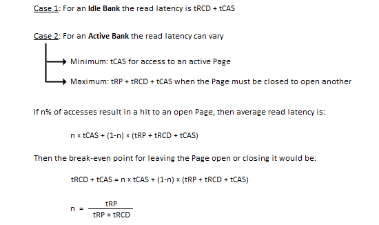
The variable n also represents the percentage of accesses to banks with open pages that must result in a page-hit access if we are to simply pace the nominal access latency that would be achieved if every read access was to an idle bank. And the only thing this depends on is the RAS Precharge delay and the Row-Column (or Command) Delay of the device in question.
You would think by working to maximize n, performance would be maximized as well. And you‘d be right. Let‘s take what we‘ve learned thus far and step it up a notch. We promise, after this you‘ll never see memory timings in the same light ever again.
Before proceeding, we‘ve prepared a video for those of you that would like to view a few simple animations meant to help visualize each transaction type:
What do you mean you‘ve never heard of Adaptive Page Management (APM) Technology? Well, that must be because Intel Marketing doesn‘t seem to feel the need to bring it up.
Simply put, Intel‘s APM determines, based on the potential implications of pending memory transactions, whether closing open pages, or allowing them to remain open longer may be beneficial to overall memory performance. In response, the memory controller may (or may not) elect to issue commands to close pages, depending on the programmed operation.
Figure 10 provides the general flow of events required to manage such a process. In our explanation we intend to introduce you to all known register settings needed to adjust the functional control policy, but first we need to detail the necessary actions, and purpose, of the design elements that make up such a mechanism. A better understanding of the underlying logic will pay dividends as you attempt to dial in measurable performance improvements through experimentation.
Per Figure 11, the Transaction Queue stores memory transactions generated by the processor. Unlike a typical First-In-First-Out (FIFO) queue with a tail, into which memory transaction may be pushed, and a head, from which memory transactions may be popped, this transaction queue is a plurality of storage elements allowing single memory transactions to be removed from the list and dispatched toward the memory in a different ordering than when originally added to the queue.
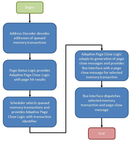
Figure 10. Generic method used by the memory controller to adaptively generate page close messages. Different system usage patterns will most likely necessitate changes to the base decision logic
Command re-ordering can improve perceived memory performance by grouping together reads/writes to a common physical page in memory, saving the time that would otherwise be needed to later re-open the same page, should a concurrent access to the same bank force it to close early. After all, the minimum delay between sequential accesses to the same open page is equal to the CAS Latency (CL or tCAS) of the device. Accessing a bank (opening a page) increases the latency of the post-interleaved operation by the Row-Column (or Command) Delay (tRCD), approximately doubling the effective data access time.
One should also appreciate that there are varying degrees of freedom when shuffling transactions in time. Like in the case of a read and write to the same memory location: the memory controller would be disallowed from moving the dependent read either ahead of or behind the associated write as the ordering must be implicitly maintained or coherency will be lost.
The Address Decoder partially decodes the memory transactions stored in the Transaction Queue as needed to determine the bank and page selected by each queued request. From there, the Bank Select messages control the multiplexers used to input the contents of a Bank Register to a comparator used to check if the selected page was also the most recently opened page for that bank (as such, each Bank Register is large enough to store n bits where each bank comprises 2n pages). A match results in the creation of a Page-Hit Result message.
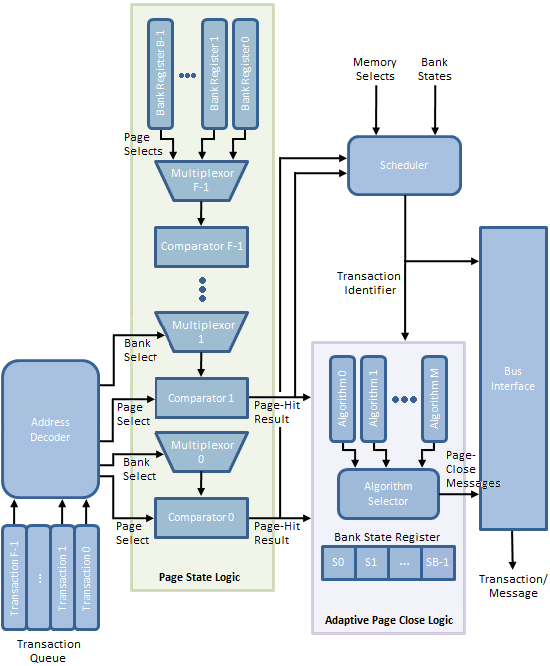
Figure 11. Our ASUS Rampage III Extreme beta BIOS includes settings used to establish the boundary regions that define when each pre-programmed Algorithm is active, the operating frequency of the policy adaption feedback loop, and the maximum single-instance lifetime for each decision to allow a page to idle open just a little longer
Triggered by the Page State Logic, the Scheduler fetches pre-identified queued memory transactions for re-ordering based on the Memory Selects (both bank and page) and the associated Page-Hit Results. An array of Bank State Registers track actions performed upon each bank by storing a state-word indicating, among other things, whether the Adaptive Page Close Logic decided to close the bank in response to a previous memory transaction to the same bank.
Finally, based on the policy instantiated by the Algorithm Selector, a Page-Close Message either is or is not generated based on the same Page-Hit Results, Bank State Registers, and Bank/Page Selects in an effort to increase the number of subsequent page-hit accesses and/or decrease the number of page-miss accesses.
An immediate and tangible gain is achieved for every successfully re-ordered transaction as a page-hit access is more efficient than a page-empty, or at worst, a page-miss. This is always the case with Core i7 and is one of this architecture‘s well known shinning points. Switch off Adaptive Page Management (disable Adaptive Page Closing in BIOS) and this is where the process ends. The page may stay open for some finite time or it may be closed right away; we‘re not sure as there‘s really no way to know without some inside help.
The Adaptive Page Close Logic must now decide whether to collect all winnings, and close the page, or let it ride, and leave it open just a while longer. While another page-hit access may yield further gains, "guessing" wrong will cause a costly page-miss access in place what would have been just a page-empty access. If only there were some way the system could measure the effectiveness of previous close decisions and then adjust policy to fit...
Surprise! The Page Manager - made up of the Page State Logic, Adaptive Page Close Logic, and Scheduler - does exactly this. How this effectiveness is measured, and how the result of that evaluation is used to adapt the decision-making process is our next topic of discussion.
标签:
原文地址:http://www.cnblogs.com/mikewolf2002/p/5179223.html