标签:des style blog http color os strong io
Methods and apparatus to provide for power consumption reduction in memories (such as cache memories) are described. In one embodiment, a virtual tag is used to determine whether to access a cache way. The virtual tag access and comparison may be performed earlier in the read pipeline than the actual tag access or comparison. In another embodiment, a speculative way hit may be used based on pre-ECC partial tag match to wake up a subset of data arrays. Other embodiments are also described.
The present disclosure generally relates to the field of computing. More particularly, an embodiment of the invention generally relates to techniques for power reduction in memories such as cache memories.
To improve performance, most modern processors include on chip cache memory. Generally, data stored in a cache is accessible may times faster than data stored in the main system memory. However, as caches become larger, they also consume a larger amount of power. Accordingly, power reduction techniques in a cache may reduce overall power consumption in a computing system.
In the following description, numerous specific details are set forth in order to provide a thorough understanding of various embodiments. However, various embodiments of the invention may be practiced without the specific details. In other instances, well-known methods, procedures, components, and circuits have not been described in detail so as not to obscure the particular embodiments of the invention. Further, various aspects of embodiments of the invention may be performed using various means, such as integrated semiconductor circuits ("hardware"), computer-readable instructions organized into one or more programs ("software"), or some combination of hardware and software. For the purposes of this disclosure reference to "logic" shall mean either hardware, software (including for example micro-code that controls the operations of a processor), or some combination thereof. Also, the use of "instruction" or "micro-operation" (which may also be referred to as "uop") herein may be interchangeable.
Some of the embodiments discussed herein provide for power reduction techniques in memory devices (such as cache memories). For example, the Level 1 Data (L1D) cache on some processor cores (such as x86 processor cores) may be virtually-indexed and physically-tagged. In a high-performance processor pipeline for a load instruction, due to tight timing constraints, in an N-way set associative cache, all N data blocks of the selected set are accessed in parallel with the tag lookup. N?1 of the N data blocks may be discarded later, constituting a waste of power. In an embodiment, this power inefficiency is mitigated without impact to the L1D cache hit latency.
In one embodiment, the physically-tagged L1D cache is augmented with a Vtag (Virtual tag) array (the highest virtual address bit in an embodiment). As discussed herein, a Vtag may be the same as a physical tag except that it consists of virtual address bit(s). In some embodiments, Vtag access and comparison are performed earlier in the read pipeline than the actual tag access/comparison, thus avoiding impact to the critical path of the L1D access. Moreover, data array accesses may be executed only for the ways whose Vtags match, as opposed to accessing all ways as is done in some of the current cache designs. For example, using the Most Significant Bit (MSB) of the virtual block address as the Vtag may reduce data array accesses for L1D reads significantly. The reason that a single bit can be so effective is that the MSB has clear virtual memory semantics, e.g., by differentiating the heap area and the stack area. The MSB bit may indicate to an incoming stack read not to pursue the ways that contain heap data, and vice versa. This solution may also be use more bits, although fewer bits may provide lower Vtag-related overhead in some embodiments. for example, in one embodiment, multiple virtual address bits may be used for the Vtag as opposed to just using the MSB. This may further reduce the number of Vtag matches in a set; therefore, avoiding more data array accesses.
Additionally, in an embodiment, to reduce power consumption, the number of Word Line (WL) firings in a memory (such as a cache memory) are reduced without any loss of performance. For example, a speculative way hit may be based on pre-ECC (Error Correction Code) partial tag match and waking up of a subset of data arrays based on the results from the match. In one embodiment, the LLC (Last Level Cache) latency is increased by one cycle (e.g., as discussed below with reference to?FIGS. 6 and 7), but the increase in turn causes saving of both leakage and dynamic power by reducing the number of data arrays that are woken up and firing only necessary word-lines.
Techniques described herein may allow for improved encryption/decryption performance in various computing devices, such as those discussed for example with reference to?FIGS. 1-12. More particularly,?FIG. 1?illustrates a block diagram of a computing system?100, according to an embodiment of the invention. The system?100?may include one or more processors102-1?through?102-N (generally referred to herein as "processors?102" or "processor?102"). The processors?102?may communicate via an interconnection network or bus?104. Each processor may include various components, some of which are only discussed with reference to processor?102-1?for clarity. Accordingly, each of the remaining processors?102-2through?102-N may include the same or similar components discussed with reference to the processor?102-1.
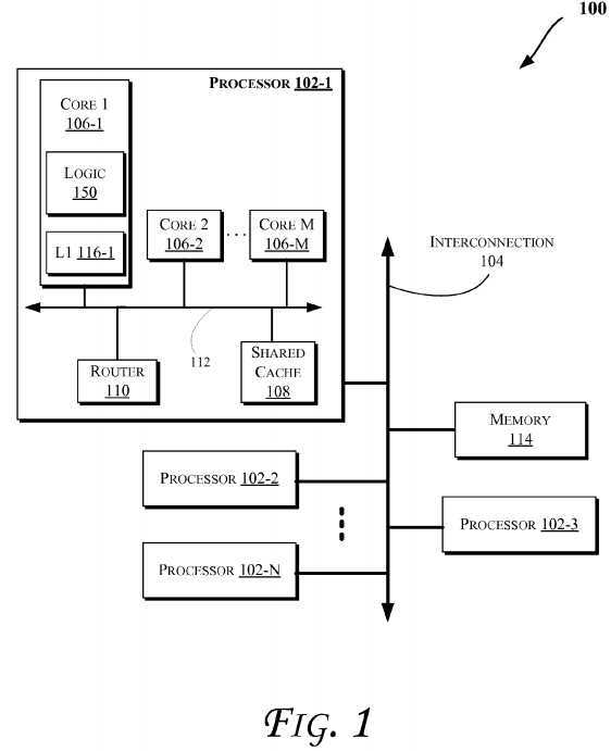
In an embodiment, the processor?102-1?may include one or more processor cores?106-1?through?106-M (referred to herein as "cores?106" or more generally as "core?106"), a shared cache?108, and/or a router?110. The processor cores?106?may be implemented on a single integrated circuit (IC) chip. Moreover, the chip may include one or more shared and/or private caches (such as cache?108), buses or interconnections (such as a bus or interconnection network?112), memory controllers (such as those discussed with reference to?FIGS. 10 and 11), or other components.
In one embodiment, the router?110?may be used to communicate between various components of the processor?102-1and/or system?100. Moreover, the processor?102-1?may include more than one router?110. Furthermore, the multitude of routers?110?may be in communication to enable data routing between various components inside or outside of the processor102-1.
The shared cache?108?may store data (e.g., including instructions) that are utilized by one or more components of the processor?102-1, such as the cores?106. For example, the shared cache?108?may locally cache data stored in a memory114?for faster access by components of the processor?102. In an embodiment, the cache?108?may include a mid-level cache (MLC) (such as a level 2 (L2), a level 3 (L3), a level 4 (L4), or other levels of cache), a last level cache (LLC), and/or combinations thereof. Moreover, various components of the processor?102-1?may communicate with the shared cache?108directly, through a bus (e.g., the bus?112), and/or a memory controller or hub. As shown in?FIG. 1, in some embodiments, one or more of the cores?106?may include a level 1 (L1) cache (116-1) (generally referred to herein as "L1 cache?116") and/or an L2 cache (not shown). As discussed herein, L1 cache may refer to an L1 Data (L1D) cache and/or L1 instruction cache.
As shown, processor core?106?may include a logic?150?to utilize a Vtag to perform a comparison earlier in the read pipeline ahead of L1D access (e.g., as will be further discussed herein with reference to?FIGS. 2A-4) and/or perform a speculative way hit based on pre-ECC partial tag match and waking up of a subset of data arrays based on the results from the match (e.g., as will be further discussed herein with reference to?FIGS. 5-9). Furthermore, even though some figures illustrate logic?150?to be inside a processor or core, logic?150?may be provided within other components of computing systems discussed herein, such as within any components of systems discussed with reference to?FIG. 1,?10, or?11.
FIG. 2A?shows one implementation of a read pipeline. Because the cache tags use physical address bits, tag comparison cannot start until a Translation Lookaside Buffer (TLB) has completed the virtual-to-physical address translation. To complete L1D read by cycle?2L (the logic low of cycle?2?at word select), the data array accesses have to start in cycle?2H (the logic high of cycle?2?at all-way data access), at which time the way selection signals are not yet available to the data array. As a result, all N ways of cache blocks in the current set are read out of the data array. On a cache hit, N?1 of the N blocks are discarded in cycle?2L.
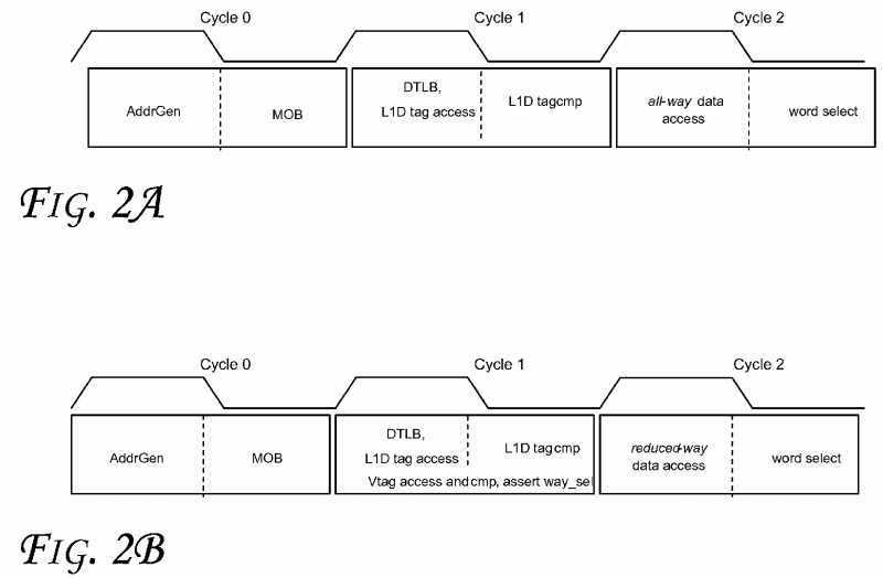
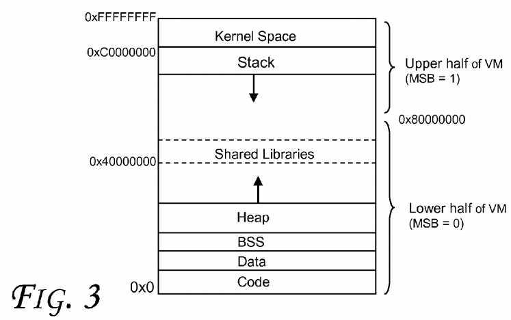
An embodiment checks a small number of virtual address bits between the memory address and the N stored cache lines in the selected set. A data block is read only if the virtual tags match. In one embodiment, each cache line with the highest bit of the 32-bit virtual address is tagged. Furthermore, the MSB of the linear address provides clear virtual memory semantics. As illustrated in?FIG. 3?(which shows a 32-bit virtual address space according to an embodiment), for the vast majority of applications, MSB of the stack area is 1 and MSB of the heap area is 0. In the extreme case when that is no longer true, the OS (Operating System) may simply disable the use of Vtag for the violating process. On 64-bit machines, the possibility of this address space shortage situation is believed to be even more remote.
In some embodiments, read hit latency is not affected. Unlike physical tags which may be only available after the TLB translation, a Vtag is ready to use after address generation, as shown in?FIG. 2B. The Vtag check signals will be available to the L1D in cycle?1L. Note that in?FIG. 2A, way selection signals cannot reach the data array in time to perform reduced-way data access.
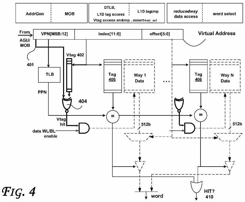
FIG. 4?illustrates a simplified organization of the optimized L1D read port, according to an embodiment. The status array is omitted for simplicity. Bold components indicate logic to utilize Vtag access and comparison path performed earlier in the read pipeline. Grey components illustrate power-saving opportunities. As shown, a virtual address is obtained from an Address Generation Unit (AGU) or Memory Ordering Buffer (MOB). As shown, the MSB?401?of the virtual address is used in conjunction with Vtag?402?to determine whether there is a Vtag hit (e.g., generated by the NOR gate?404). The Vtag hit signal is compared with entries from tags?406?and?408?to determine whether a hit?410?has occurred.
In some embodiments, a stack variable and a heap variable may share a same physical memory block, e.g., as a result of the mmap( ) system call in accordance with at least one instruction set architecture. Vtag would give us a false miss in the L1D. If the L1D cache line is in M (modified) state, the miss will cause obsolete data from low-level memory to overwrite the dirty copy in L1D. Intentional virtual address aliasing is generally rare in practice. We only need to ensure program correctness when a false miss occurs. There are several solutions. A software solution is for the OS to disable Vtag usage for the current process when an alias mapping is created in the page table. A hardware solution is to nuke the consequent L1D miss request (in cycle?2?of?FIG. 2) and re-execute data array access, if physical tag comparison does not agree with the Vtag check result. This one-cycle penalty only affects an aliased L1D read, and does not affect L1D hit or miss latencies for non-aliasing cases.
Moreover, some of embodiments discussed herein do not serialize the cache access process, which does not impact cache access time. Also, some of the embodiments discussed herein are oblivious of past accesses, and are not speculative in nature. Further, in one embodiment, multiple virtual address bits may be used for Vtag as opposed to just using the MSB. This may further reduce the number of Vtag matches in a set; therefore, avoiding more data array accesses. In an embodiment, instruction linear address bits may be used to optimize L1 instruction cache power. In the latter case, instruction linear address bits may differentiate user versus kernel code, and/or application versus shared library. Additionally, while some embodiments are discussed with reference to L1D herein, techniques discussed herein may be applied to other levels of cache (such as those discussed with reference to?FIG. 1, including for example, L2, L3, etc.).
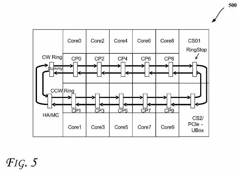
FIG. 5?illustrates a physically distributed and logically shared cache memory subsystem in a multi-core computing system500, according to an embodiment. As shown, system?500?includes multiple slices of caches CP0?to CP9?(e.g., physically partitioned and logically shared) coupled through a bi-directional ring architecture (where each coupling shown with a unidirectional arrow may be a unidirectional point-to-point coupling). As shown, each pair of caches may be coupled with two unidirectional couplings which together form a clockwise (CW) communication ring and the counter clockwise (CCW) communication ring. A homing agent (HA)/memory controller (MC) may be present in the system, along with a ring stop (CS01) and a PCIe (PCI express) UBox (CS2). As illustrated the rings may also be coupled to a dummy agent.
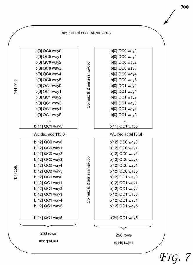
Referring to?FIG. 6, an LLC data array organization is shown, according to an embodiment. Even though an LLC is discussed, the embodiments are applicable to other cache levels such as those discussed with reference to?FIG. 1, for example. The LLC may include 192 data sub-arrays (see, e.g.,?FIG. 7?for details of a sample sub-array), each storing 16K bits (3 MB cache size). 3 MB data cache is assumed to be organized as 2K sets with 24-ways per set. STCV (State and Core Valid) arrays which couple various sub-arrays may store the state-bits and core-valid bit vector for all the cache lines. Core-valid vector is a presence vector that indicates which of the cores have a copy of a given cache line. In the baseline case (without the proposed power reduction techniques described herein), all the 48 sub-arrays (corresponding to all the 24-ways) are woken up and 48 WLs are fired. Then, the way hit information is used to column multiplex the bits in the SSAs to the sense amps. The way hit information is also used to generate sense amp enables in the 12 sub arrays corresponding to way-hit. Thus, the wakeup and firing of WL in the other 36 sub arrays contributes wasteful power. In-order to selectively wake-up 12 word lines corresponding to the select group of 6-ways, LLC controller has to wait for tag-match and tag-ECC correction to complete. For meeting RAS (Reliability, Availability, and Serviceability) requirements, server products are generally required to implement DECTED (Double Error correction Triple Error Detection) in the data arrays and SECDED (Single Error correction and Double Error Detection) in the tag arrays. The tag-ECC operation consumes an additional cycle. Generally, waiting for complete tag match and tag-ECC checking to complete to wake up and fire data sub-arrays adds two cycles to LLC-hit latency, resulting in loss of performance. Thus, there is a trade-off between less performance (two cycle increase in LLC latency) and higher power (waking up and firing of all the 48 WLs corresponding to 24-ways).
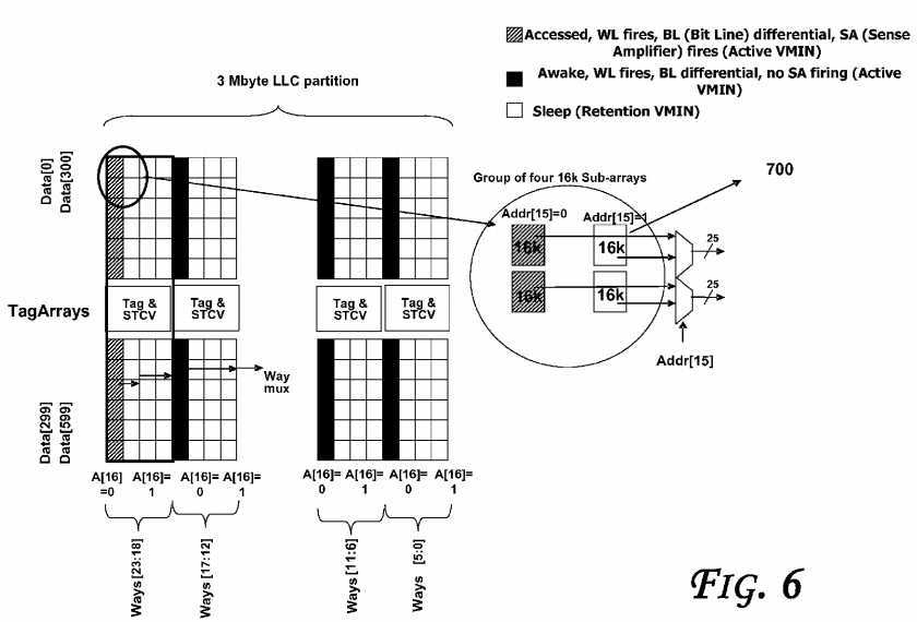
In some embodiments, each of the LLC slices, LLC data arrays may be implemented as SSAs (Small Signal Arrays) with embedded sleep circuitry to save power. To read a cache line, the appropriate data sub-arrays are woken up, the corresponding WLs (word lines) are fired, and sense amps enabled to output the data from the memory cells. Also, as shown in?FIG. 6, the LLC partitions may have one or more of three distinct modes: accessed (e.g., corresponding to an energizing of sense amplifiers (SAs) of the data arrays with WL firing and BL (Bit Line) differential (e.g., cells at active Vmin)), awake (e.g., with WL firing, BL differential and no SA firing (e.g., cells at active Vmin)), and/or sleep (e.g., retention at minimum voltage level (e.g., cells at retention Vmin)).
Referring to Table 1 below (which lists some sample performance vs. power trade-off options), at row 2, to reduce power consumption, the number of word-line (WL) firings in a memory (such as an LLC) are reduced without any loss of performance (no increase in LLC access latency). At row 3, the LLC hit latency is increased by one cycle, but the increase in turn causes saving of both leakage and dynamic power by reducing the number of data arrays that are woken up and firing only necessary word-lines.
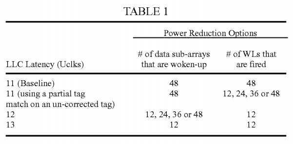
In one embodiment, power optimization may be achieve by using a partial tag match based on the pre-ECC (un-corrected) tag and firing only a subset of WLs instead of all the 48. More specifically, the un-corrected pre-ECC tag may be split into Odd-bits and Even-bits in some embodiments. The partial tag match will be true, if either all the odd-bits match with the corresponding bits of the address tag or all the even-bits match with the corresponding bits of the address tag. If the partial tag match is false, then the real tag match (using all the bits of ECC-corrected tag) would be false (by definition) too. However, if the partial tag match is true, then the actual tag match could be either true or false. Thus, firing WLs based on partial tag match could result in firing more WLs than necessary. As reflected in row 2 of Table 1, the number of WLs fired could be 12, 24, 36 or 48 (depending on the workload).
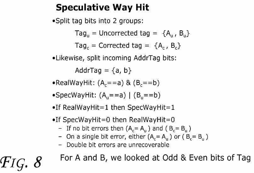
The pseudo code shown in?FIG. 8?provides sample details of speculative way hit scheme, according to an embodiment. As shown, tag bits are split into two groups. The incoming address tag bits may also be split as shown. Next, real way hit and speculative way hit are determined. If the real way hit is equal to one (indicating an actual hit) then the speculative way hit is set to one. If speculative way hit is zero (indicating no speculative hit), then the real way hit is set to zero. Furthermore, if no-bid errors are detected, the split tag bit groups are updated. For a single bit error, the split tag bit groups are updated as shown. In one embodiment, the double bit errors are unrecoverable. As will be further discussed herein, e.g., with respect to?FIG. 9, for A and B, odd and even bits of tag may be considered.
More specifically,?FIG. 9?illustrates a flow diagram of a method?900?using a speculative way hit scheme to reduce power according to an embodiment. In some embodiments, one or more components of?FIG. 1-8?or?10-12?may be used to perform one or more operations of method?900. At an operation?902, a cache access request is received. Operations?904and?906, respectfully, extract the tag corresponding to the cache access request and use a set index to look up in tag array corresponding to the cache access request. As shown, operations?904?and?906?may be performed in parallel in one embodiment. An operation?908?reads the tags based on the set index. Operations?910?and?912?split the tags into halves914?which are then compared operations?916?and?918. They sub-array speculative wake up vector is then generated (at operation?920) based on the output of the comparisons?916?and?918?(e.g., by logically or-ing the outputs of the comparisons916?and?918).
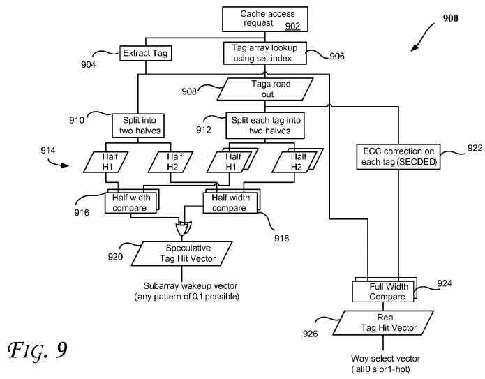
As illustrated in?FIG. 9, at operation?922, ECC correction may be performed on each tag (e.g., using SECDED as discussed above). The output of the ECC correction?922?and tag extraction?904?may be used to perform a full width compare?924, which in turn provides a real tag hit vector?926?for a real/actual way selection vector. Moreover, even thoughFIG. 9?discusses halving the tags, other portions may also be used, such as quarter, etc.
Accordingly, some embodiments may reduce significant amount of the power at the overall chip level with no or marginal loss in performance. These savings in power could in turn be used to boost the processor core frequency to improve the performance of the overall chip. Also, a speculative cache way hit of a cache memory may be determined based on a pre ECC partial tag match (e.g., where tags are split as shown in?FIG. 9, for example).
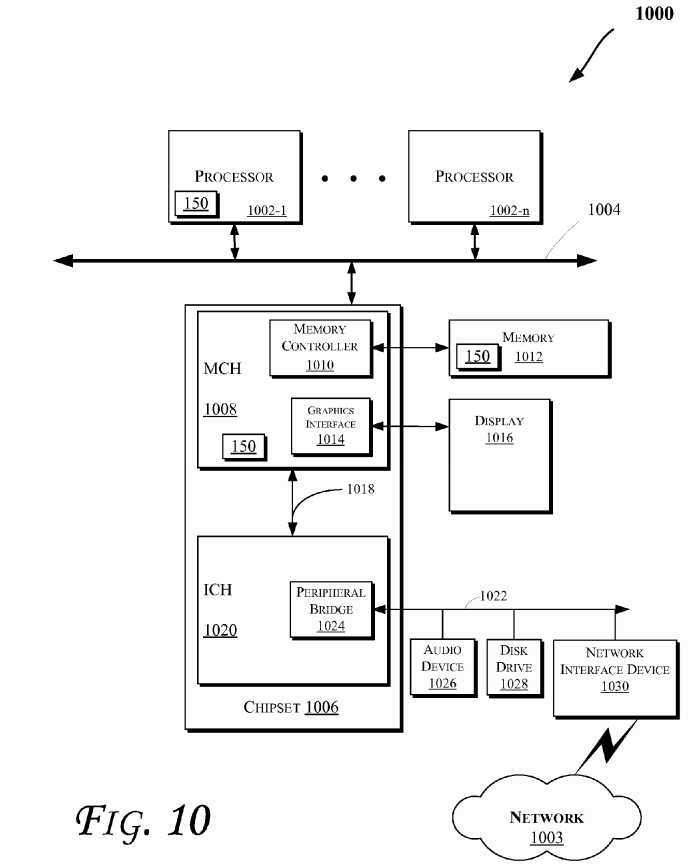
FIG. 10?illustrates a block diagram of an embodiment of a computing system?1000. In various embodiments, one or more of the components of the system?1000?may be provided in various electronic devices capable of performing one or more of the operations discussed herein with reference to some embodiments of the invention. For example, one or more of the components of the system?1000?may be used to perform the operations discussed with reference to?FIGS. 1-9. Also, various storage devices discussed herein (e.g., with reference to?FIGS. 1?and/or?11) may be used to store data, operation results, etc. Also, various components of system?1000?may include the logic?150. Even though presence of logic?150?is shown in some components of system?1000, logic?150?may be present in more or less components.
Moreover, the computing system?1000?may include one or more central processing unit(s) (CPUs)?1002?or processors that communicate via an interconnection network (or bus)?1004. The processors?1002?may include a general purpose processor, a network processor (that processes data communicated over a computer network?1003), or other types of a processor (including a reduced instruction set computer (RISC) processor or a complex instruction set computer (CISC)). Moreover, the processors?1002?may have a single or multiple core design. The processors?1002?with a multiple core design may integrate different types of processor cores on the same integrated circuit (IC) die. Also, the processors?1002?with a multiple core design may be implemented as symmetrical or asymmetrical multiprocessors. Moreover, the operations discussed with reference to?FIGS. 1-9?and/or?11-12?may be performed by one or more components of the system?1000.
A chipset?1006?may also communicate with the interconnection network?1004. The chipset?1006?may include a memory control hub (MCH)?1008. The MCH?1008?may include a memory controller?1010?that communicates with a memory?1012. The memory?1012?may store data, including sequences of instructions that are executed by the CPU?1002, or any other device included in the computing system?1000. In one embodiment of the invention, the memory?1012?may include one or more volatile storage (or memory) devices such as random access memory (RAM), dynamic RAM (DRAM), synchronous DRAM (SDRAM), static RAM (SRAM), or other types of storage devices. Nonvolatile memory may also be utilized such as a hard disk. Additional devices may communicate via the interconnection network?1004, such as multiple CPUs and/or multiple system memories.
The MCH?1008?may also include a graphics interface?1014?that communicates with a display?1016. In one embodiment of the invention, the graphics interface?1014?may communicate with the display?1016?via an accelerated graphics port (AGP). In an embodiment of the invention, the display?1016?may be a flat panel display that communicates with the graphics interface?1014?through, for example, a signal converter that translates a digital representation of an image stored in a storage device such as video memory or system memory into display signals that are interpreted and displayed by the display?1016. The display signals produced by the interface?1014?may pass through various control devices before being interpreted by and subsequently displayed on the display?1016.
A hub interface?1018?may allow the MCH?1008?and an input/output control hub (ICH)?1020?to communicate. The ICH?1020may provide an interface to I/O devices that communicate with the computing system?1000. The ICH?1020?may communicate with a bus?1022?through a peripheral bridge (or controller)?1024, such as a peripheral component interconnect (PCI) bridge, a universal serial bus (USB) controller, or other types of peripheral bridges or controllers. The bridge?1024may provide a data path between the CPU?1002?and peripheral devices. Other types of topologies may be utilized. Also, multiple buses may communicate with the ICH?1020, e.g., through multiple bridges or controllers. Moreover, other peripherals in communication with the ICH?1020?may include, in various embodiments of the invention, integrated drive electronics (IDE) or small computer system interface (SCSI) hard drive(s), USB port(s), a keyboard, a mouse, parallel port(s), serial port(s), floppy disk drive(s), digital output support (e.g., digital video interface (DVI)), or other devices.
The bus?1022?may communicate with an audio device?1026, one or more disk drive(s)?1028, and a network interface device1030, which may be in communication with the computer network?1003. In an embodiment, the device?1030?may be a NIC capable of wireless communication. Other devices may communicate via the bus?1022. Also, various components (such as the network interface device?1030) may communicate with the MCH?1008?in some embodiments of the invention. In addition, the processor?1002?and the MCH?1008?may be combined to form a single chip. Furthermore, the graphics interface?1014may be included within the MCH?1008?in other embodiments of the invention.
Furthermore, the computing system?1000?may include volatile and/or nonvolatile memory (or storage). For example, nonvolatile memory may include one or more of the following: read-only memory (ROM), programmable ROM (PROM), erasable PROM (EPROM), electrically EPROM (EEPROM), a disk drive (e.g., 1028), a floppy disk, a compact disk ROM (CD-ROM), a digital versatile disk (DVD), flash memory, a magneto-optical disk, or other types of nonvolatile machine-readable media that are capable of storing electronic data (e.g., including instructions). In an embodiment, components of the system?1000?may be arranged in a point-to-point (PtP) configuration such as discussed with reference to?FIG. 11. For example, processors, memory, and/or input/output devices may be interconnected by a number of point-to-point interfaces.
More specifically,?FIG. 11?illustrates a computing system?1100?that is arranged in a point-to-point (PtP) configuration, according to an embodiment of the invention. In particular,?FIG. 11?shows a system where processors, memory, and input/output devices are interconnected by a number of point-to-point interfaces. The operations discussed with reference toFIG. 1-10?or?12?may be performed by one or more components of the system?1100. Also, various components of system1100?may include the logic?150. Even though presence of logic?150?is shown in some components of system?1100, logic150?may be present in more or less components.
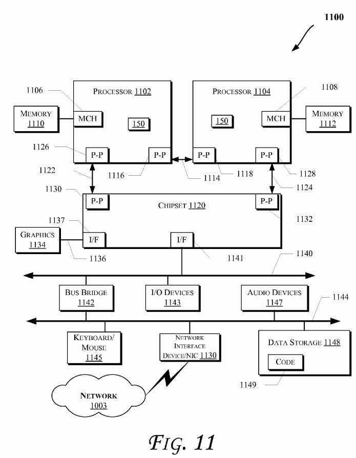
As illustrated in?FIG. 11, the system?1100?may include several processors, of which only two, processors?1102?and?1104are shown for clarity. The processors?1102?and?1104?may each include a local memory controller hub (MCH)?1106?and1108?to couple with memories?1110?and?1112. The memories?1110?and/or?1112?may store various data such as those discussed with reference to the memory?1012?of?FIG. 10.
The processors?1102?and?1104?may be any suitable processor such as those discussed with reference to the processors1002?of?FIG. 10. The processors?1102?and?1104?may exchange data via a point-to-point (PtP) interface?1114?using PtP interface circuits?1116?and?1118, respectively. The processors?1102?and?1104?may each exchange data with a chipset1120?via individual PtP interfaces?1122?and?1124?using point to point interface circuits?1126,?1128,?1130, and?1132. The chipset?1120?may also exchange data with a high-performance graphics circuit?1134?via a high-performance graphics interface?1136, using a PtP interface circuit?1137.
At least one embodiment of the invention may be provided by utilizing the processors?1102?and?1104. For example, the processors?1102?and/or?1104?may perform one or more of the operations of?FIG. 1-10?or?12. Other embodiments of the invention, however, may exist in other circuits, logic units, or devices within the system?1100?of?FIG. 11. Furthermore, other embodiments of the invention may be distributed throughout several circuits, logic units, or devices illustrated in?FIG. 11.
The chipset?1120?may be coupled to a bus?1140?using a PtP interface circuit?1141. The bus?1140?may have one or more devices coupled to it, such as a bus bridge?1142?and I/O devices?1143. Via a bus?1144, the bus bridge?1143?may be coupled to other devices such as a keyboard/mouse?1145, the network interface device?1130?discussed with reference toFIG. 11?(such as modems, network interface cards (NICs), or the like that may be coupled to the computer network?1003), audio I/O device, and/or a data storage device?1148. The data storage device?1148?may store code?1149?that may be executed by the processors?1102?and/or?1104.
FIG. 12?illustrates a block diagram of portions of a processor core and other components of a computing system, according to an embodiment of the invention. In an embodiment, at least some of processors discussed herein (e.g., with reference toFIG. 1,?10, or?11) may include one or more of the component of the processor core?106?shown in?FIG. 12. Also, a processor may include a single or multi-core?106, which may be homogeneous/symmetric or heterogeneous/asymmetric, etc. such as discussed herein, e.g., with reference to?FIG. 1,?10, or?11. In one embodiment, the arrows shown in?FIG. 12illustrate the flow direction of instructions through the core?106. One or more processor cores (such as the processor core106) may be implemented on a single integrated circuit chip (or die) such as discussed with reference to?FIG. 1. Moreover, the chip may include one or more shared and/or private caches (e.g., cache?108?of?FIG. 1), interconnections (e.g., interconnections?104?and/or?112?of?FIG. 1), memory controllers, or other components.
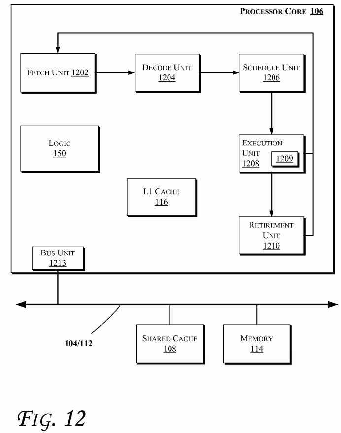
As illustrated in?FIG. 12, the processor core?106?may include a fetch unit?1202?to fetch instructions for execution by the core106. The instructions may be fetched from any storage devices such as the memory?114?and/or the memory devices discussed with reference to?FIG. 10?or?11. The core?106?may optionally include a decode unit?1204?to decode the fetched instruction. In an embodiment, the decode unit?1204?may decode the fetched instruction into a plurality of uops (micro-operations). Some embodiments of the processor core?106?may not include decode unit?1204. Hence, the core?106?may process instructions without decoding them. Additionally, the core?106?may include a schedule unit?1206. The schedule unit1206?may perform various operations associated with storing decoded instructions (e.g., received from the decode unit1204) until the instructions are ready for dispatch, e.g., until all source values of a decoded instruction become available.
In one embodiment, the schedule unit?1206?may schedule and/or issue (or dispatch) decoded instructions to an execution unit?1208?for execution. The execution unit?1208?may execute the dispatched instructions after they are dispatched (e.g., by the schedule unit?1206) and, if applicable, decoded (e.g., by the decode unit?1204). In an embodiment, the execution unit1208?may include more than one execution unit, such as one or more memory execution units, one or more integer execution units, one or more floating-point execution units (1809), or other execution units. The execution unit?1208?may also perform various arithmetic operations such as addition, subtraction, multiplication, and/or division, and may include one or more an arithmetic logic units (ALUs). In an embodiment, a co-processor (not shown) may perform various arithmetic operations in conjunction with the execution unit?1208.
Further, the execution unit?1208?may execute instructions out-of-order. Hence, the processor core?106?may be an out-of-order processor core in one embodiment. The core?106?may also include a retirement unit?1210. The retirement unit?1210may retire executed instructions (e.g., in order) after they are committed. In an embodiment, retirement of the executed instructions may result in processor state being committed from the execution of the instructions, physical registers used by the instructions being de-allocated, etc.
The core?106?may further include the logic?150?(such as the logic?150?discussed with respect to any of the previous figures). Additionally, the core?106?may include a bus unit?1213?to allow communication between components of the processor core106?and other components (such as the components discussed with reference to?FIG. 1,?10, or?11) via one or more buses (e.g., buses?104?and/or?112).
SRC=http://www.google.com/patents/US20110161595
Cache memory power reduction techniques,布布扣,bubuko.com
Cache memory power reduction techniques
标签:des style blog http color os strong io
原文地址:http://www.cnblogs.com/coryxie/p/3876832.html