标签:des style blog http color os io strong
Within a multi-processing system including a plurality of processor cores?4, 6operating in accordance with coherent multi-processing, each of the cores includes a cache memory?10, 12?storing local copies of data values from a coherent memory region. The respective processor cores may be placed into apower?saving mode in which they are non-operative whilst the cache memory remains responsive to coherency management requests such that the system as a whole can continue to operate and manage coherency.
This invention relates to data processing systems. More particularly, this invention relates to data processing systems including multiple processor cores performing respective data processing operations and sharing access to a coherent memory region.
It is known to provide data processing systems including two or more processor cores which operate in a coherent multi-processing mode in which they share access to a coherent memory region. In such systems the different processor cores typically perform respective data processing operations in parallel to achieve an overall desired processing result.
An example of a coherent multi-processing system is the IBM370 system and SPARC multi-processor system. Such coherent multi-processing systems are high performance systems where?power?efficiency and?power?consumption is of little concern and the main objective is maximum processing speed.
An important consideration in coherent multi-processing systems is the management of coherency between cached copies of data values being held by different processor cores. It is known to provide memory access control units coupled to the processor cores which serve to perform coherency management operations to avoid situations such as a locally cached data value which is out-of-date being incorrectly used by a processor core when elsewhere within the coherent multi-processing system there is a more up-to-date version of that data value which should instead be used.
Viewed from one aspect the present invention provides apparatus for processing data, said apparatus comprising:
The invention recognises that within coherent multi-processing systems containing cached copies of a data value then advantageous?power?savings may be made whilst preserving the ability to maintain coherency by use of a technique whereby a processor core is powered down and made inactive whilst its cache memory storing the data values for which coherency needs to be maintained remains active and services coherency management operations generated by a memory access control unit without requiring the processor core itself to remain active. This technique runs counter to the normal practice in the field whereby a cache memory is typically powered down and rendered inactive when its associated processor core is powered down and rendered inactive. Maintaining the?power?to the cache has the advantages that?power?down of the core is speed up since there is no need to flush the cache, relatively fast access by other cores to the cached memory may be achieved avoiding relatively slow main memory accesses and upon wake up of the core there is a probability that required data will still be cached avoiding the need for a relatively slow refill.
A particularly convenient way of rendering the processor core inactive is to gate its clock.
It will be appreciated that the coherency management operations which need to be supported by the cache memory whilst the processor core is powered down can take a variety of different forms. In preferred embodiments of the present invention these coherency management operations include a copy coherence management request to trigger return to the memory access management unit of a copy of a data value stored within the cache memory, a status change coherency management request from the memory access management unit serving to change a status value associated with a data value that is stored within the cache memory, and a clean coherency management request to trigger the cache memory to flush a dirty value stored therein to a main coherent memory.
Whilst it will be appreciated that the processor core advantageously saves?powerby being moved into its inactive state, it is important that it should be quick and easy to reactivate the processor core and accordingly preferred embodiments are ones in which the processor core is responsive to a received interrupt signal to return to the active powered state from the inactive?power?saving state.
Whilst it will be appreciated that the present technique may be advantageously used when only some of the processor cores have associated cache memories which remain active when their processor core is powered down, the invention is particularly suited for use in systems in which all of the processor cores have associated cache memories and all of these cache memories are ones which can remain active when their associated processing core is inactive.
Whilst it will be appreciated that the present technique may be embodied in a system in which the processor cores, cache memories, memory access control unit, etc are formed upon different integrated circuits or combinations of integrated circuits, the invention is particularly well suited when these elements are formed on a single integrated circuit.
Viewed from another aspect the present invention provides a method of processing data, said method comprising the steps of:
The above, and other objects, features and advantages of this invention will be apparent from the following detailed description of illustrative embodiments which is to be read in connection with the accompanying drawings.
FIG. 1?schematically illustrates an integrated circuit?2?containing a plurality of microprocessor cores?4,?6,?8, each with an associated cache memory?10,?12,?14. The processor cores?4,?6,?8?are connected by respective memory buses AHB, CCB to a memory management access unit?16?(also called a snoop control unit). A peripheral device?18?is provided as a private peripheral connected to one of the processor cores?4.
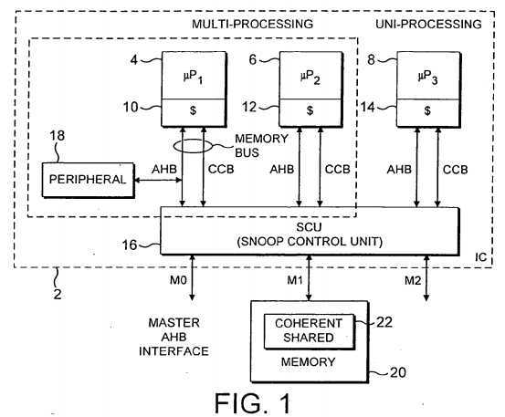
The integrated circuit?2?is coupled to a memory?20?by one of several possible master AHB ports. The memory?20?contains a coherent shared region?22. Memory may be configured and used as non-coherent shared memory when more than one processor has access to it, e.g. a general purpose processor core and a specialist DSP core may share access to a common memory region with no control of coherency being performed. Coherent shared memory is distinguished from non-coherent shared memory in that in coherent shared memory the mechanisms by which that memory is accessed and managed are such as to ensure that a write or a read to a memory location within that coherent shared region will act upon or return the current and most up-to-date version of the data value concerned. Thus, coherent shared memory is such that if one processor core makes a change to a data value within the coherent shared region, then another processor core will read that up-to-date data value when it seeks to access that data value. Furthermore, a write to a data value within the coherent memory region?22?will force a change in other stored copies of that data value, at least to the level of ensuring that out-of-date copies are marked as invalid and so subsequently not used inappropriately.
In the system of?FIG. 1, the snoop control unit?16?is responsible for managing access to the memory?20, and the coherent shared memory region?22?in particular. The snoop control unit?16?keeps track of which processor cores?4,?6?that are acting in a coherent multi-processing mode are currently holding local copies of a data value from the coherent memory region?22within their cache memories?10,?12. Coherency management is in itself a known technique. Descriptions of such techniques may be found for example within the Western Research Laboratory Research Report 95/7 entitled "Share Memory Consistency Models: A Tutorial" by Sarita V. Adve and Kourosh Gharachorloo; University of Wisconsin—Madison Computer Sciences Technical Report/902 December 1989; "Weak Ordering—A New Definition And Some Indications" by Sarita V. Adve and Mark D Hill; and "An Implementation Of Multi Processor Linux" by Alan Cox, 1995. Whilst coherent multi-processing itself is an established technique, the provision of such capability with reduced hardware complexity overhead, backward compatibility and configuration flexibility is a significant challenge.
FIG. 2?illustrates the memory bus between the processor cores?4,?6,?8?and the snoop control unit?16?in more detail. In particular, this memory bus is formed of an AHB bus (AMBA High-Performance Bus) in parallel with a coherency control bus (CCB). The AHB bus has the standard form as is known from and described in documentation produced by ARM Limited of Cambridge, England. This AHB bus is a uni-processing bus with the normal capabilities of operating with processor cores performing uni-processing (or non-coherent multi-processing such as a core and a DSP accessing a shared non-coherent memory). The AHB bus does not provide capabilities for coherent multi-processing. Private peripheral devices, such as a peripheral device?18?as illustrated in?FIG. 1, may be connected to this bus without modification providing they do not need to access the coherent multi-processing capabilities of the system. This provides advantageous backward compatibility with existing peripheral designs.
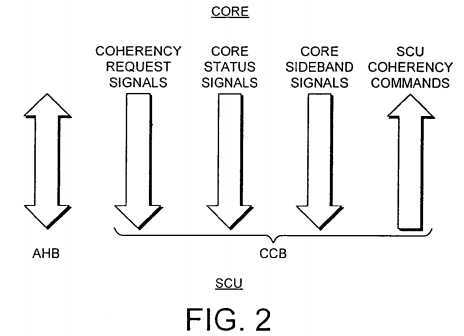
The coherency control bus CCB can be considered to provide a number of respective channels of communication between the attached processor core?4,?6?and the snoop control unit?16. In particular, the core may generate coherency request signals, core status signals and core side band signals which are passed from the processor core?4,?6?to the snoop control unit?16. The snoop control unit?16?can generate coherency commands that are passed from the snoop control unit?16?to the respective processor core?4,?6.
The CCB in particular is used to augment signal values on the AHB to provide additional information from the core?4,?6?to the snoop control unit?16?characterising the nature of a memory access being requested such that the coherency implications associated with that memory access request can be handled by the snoop control unit?16. As an example, line fill read requests for the cache memory?10,?12?associated with a coherent multi-processing core?4,?6?may be augmented to indicate whether they are a simple line fill request or a line fill and invalidate request whereby the snoop control unit?16?should invalidate other copies of the data value concerned which are held elsewhere. In a similar way, different types of write request may be distinguished between by the coherency request signals on the CCB in a manner which can then be acted upon by the snoop control unit?16.
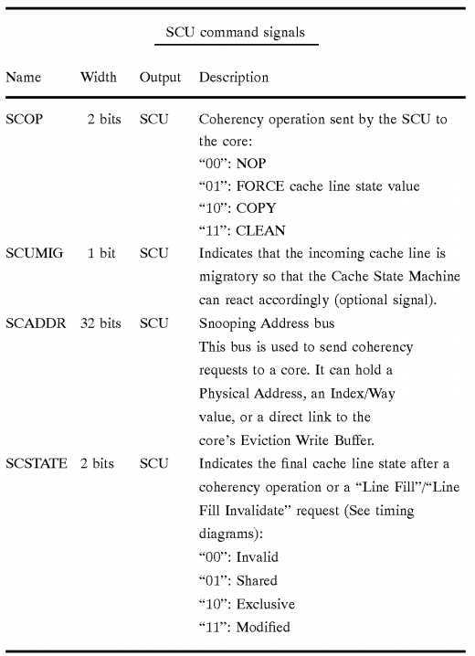
The core status signals pass coherency related information from the core to the snoop control unit such as, for example, signals indicating whether or not a particular core is operating in a coherent multi-processing mode, is ready to receive a coherency command from the snoop control unit?16, and does or does not have a data value which is being requested from it by the snoop control unit?16. The core sideband signals passed from the core to the snoop control unit?16?via the CCB include signals indicating that the data being sent by the core is current valid data and can be sampled, that the data being sent is "dirty" and needs to be written back to its main stored location, and elsewhere as appropriate, that the data concerned is within an eviction write buffer and is no longer present within the cache memory of the core concerned, and other signals as may be required. The snoop control unit coherency commands passed from the snoop control unit?16?to the processor core?4,?6?include command specifying operations relating to coherency management which are required to be performed by the processor core?4,?6?under instruction of the snoop control unit?16. As an example, a forced change in the status value associated with a data value being held within a cache memory?10,?12?of a processor core?4,?6?may be instructed such as to change that status from modified or exclusive status to invalid or shared in accordance with the applied coherency protocol. Other commands may instruct the processor core?4,?6?to provide a copy of a current data value to the snoop control unit?16?such that this may be forwarded to another processor core to service a memory read request, from that processor core. Other commands include, for example, a clean command.
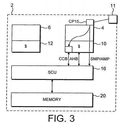
FIG. 3?illustrates a section of an integrated circuit?2?according to an embodiment of the invention. The integrated circuit?2, comprises a memory access control unit?16, (often referred to as the snoop control unit or memory management access unit), a memory?20?and a plurality of processor cores?4,?6. The processor cores include processor core?4?that is configurable to operate either in non-coherent processing mode or in coherent multi-processing mode. The other processor cores (not all shown in?FIG. 3) may be multi-processor cores, non-coherent processor cores or they may be like processor core?4?configurable to operate as either.
Processor cores operating in coherent multi-processing mode have access to a shared memory region, this region being cachable by the cores operating in coherent multi-processing mode and a defined portion of memory?20. Processor cores operating in non-coherent mode do not access coherent shared memory region and their caches do not mirror any data contained in these regions.
Although memory?20?is shown as a block on the integrated circuit?2, this is purely for ease of illustration and in reality memory?20?may include a variety of data stores on and/or off the integrated circuit and also the caches of the processor cores.
Processor core?4?has an associated cache memory?10?and a mode control parameter storage element, which in this embodiment is part of the CP15 register. The mode control parameter controls the processor core to operate either in non-coherent processing mode or in coherent multi-processing mode. The parameter may be set in a variety of ways including in response to a software command from an application or operating system, or it may be hardware controlled by a signal on an external pin?11.
As in the other embodiments processor core?4?communicates with the snoop control unit via a bus. This bus is divided into two portions, the main or AHB portion and the multi-processing or CCB (coherency control bus) portion. The main portion is used to transmit memory access signals from the processor core to the snoop control unit and from the snoop control unit to the core, the additional portion is used for additional information related to coherency management operations.
In operation when the mode control parameter is set to indicate that the processor core is to operate in non-coherent processing mode, the core acts in response to this signal to de-activate the CCB. This means that memory access signals are sent by the AHB bus alone and have no additional coherency related data attached to them. As no additional coherency information is received by the snoop control unit?16?it performs no coherency operations on the memory access request but simply directs the memory access request to the relevant portion of memory?20.
As can be seen from?FIG. 3, in addition to controlling the core?4?to de-activate the CCB, the mode control parameter is sent directly to the snoop control unit?16?as an?SMP/AMP signal. As in this case the mode control parameter is set to indicate that the processor core?4?is operating in non-coherent processing mode, the signal received by the snoop control unit?16indicates that the cache?10?of processor core?4?is not mirroring any shared memory. Cache memory?10?is therefore not relevant to the snoop control unit?16?when it is servicing memory access requests from other cores and the snoop control unit?16?therefore ignores cache memory?10?when servicing memory access requests from other processor cores.
When the mode control parameter is set to indicate that processor core?4?is to operate in coherent multi-processing mode, the CCB bus is not automatically de-activated. In this circumstance the core may produce additional information to describe a particular memory access request and act to transmit the memory access request on the AHB bus and the additional data on the CCB bus. The receipt of the additional information on the CCB bus indicates to the snoop control unit that processor core?4?is operating in coherent multi-processing mode and that coherency management operations need to be performed. In some circumstances the memory access request is such that although the core is operating in coherent multi-processing mode it knows that there are no coherency problems associated with this particular request. In these circumstances, for example, where the core knows that the latest version of the data it needs to read is in its own cache, the core acts to de-activate the CCB as in the non-coherent processor mode and no additional information is sent with the memory access request. In this case as in the non-coherent processing mode example the snoop control unit knows that no coherency management operations need to be performed and thus it simply directs the memory access request to the memory location indicated.
As in this case the mode control parameter is set to indicate coherent multi-processing mode, the cache?10?of processor core?4?mirrors part of the shared memory accessible to other processor cores?6?operating in coherent multi-processing mode and is thus relevant to the snoop control unit?16?servicing memory access requests from coherent multi-processing mode processors. As the snoop control unit?16?receives a signal giving the value of the mode control parameter it is?awareof this and as such does not ignore the cache?10?of core?4?when servicing memory access requests from other processor cores operating in coherent multi-processing mode.
FIG. 4?shows an alternative embodiment where the processor cores?4,?6,?8?are all configurable to operate either in multi-processing or in non-coherent processing mode. In this embodiment the mode control parameters are not stored on the processor cores themselves but are rather stored on the snoop control unit?16. In the embodiment shown these signals are sent to the cores and can be used by the cores, as in the embodiment illustrated in?FIG. 3, to disable the CCB if they indicate the processor core to be operating in non-coherent processor mode. As they are stored on the snoop control unit16, the snoop control unit has access to them and uses them to determine which processor core caches it needs to access when servicing memory access requests from coherent multi-processing mode processor cores.
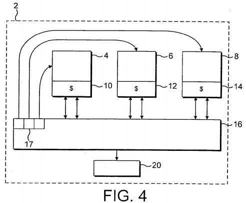
Although the two embodiments illustrated have shown the control parameters stored either in the configurable core?4?or on the snoop control unit?16, it would be possible to store these parameters elsewhere on the integrated circuit?2. In all of these embodiments the control parameters may be set in a variety of ways including in response to a software command from an application or operating system, or they may be hardware controlled by a signal on an external pin (not shown).
FIG. 5?schematically illustrates a processor core?4?with an attached cache memory?10. This cache memory?10?is a 4-way physically addressed cache memory. The cache memory?10?is supplied with its own clock signal. The clock signal which is supplied to the processor?4?may be gated off by a control gate?24?whilst the clock continues to be supplied to the cache memory?10. Thus, the processor core?4?may be stopped and placed into a?power?saving mode by gating off its clock with the control gate?24. A status flag within a core configuration coprocessor CP15 is used to switch the control gate?24between allowing the clock signal to pass and gating off the clock signal. One type of WFI (wait for interrupt) instruction is used to trigger setting of this status flag and gating of the core clock while the cache clock remains active. Another type of WFI instruction may be used to gate the clock to both the core and the cache.
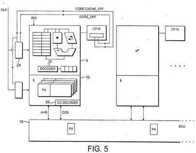
Within the cache memory?10, a coherency command decoder?26?is provided and is responsive to coherency commands passed via the CCB from the snoop control unit?16. These coherency commands include forcing a change in status associated with a data value held within the cache memory?10, returning a copy of a data value held or cleaning a data value held as instructed by the snoop control unit?16. Thus, whilst the processor core?4?may be placed into a?power?saving mode to reduce overall system?power?consumption, the cache memory?10?can remain responsive to coherency management requests issued by the snoop control unit?16?and directed to it via the CCB. This enables significant?power?saving whilst not compromising the coherency management.
A further description of the multi-processor architecture in general is given in the following:
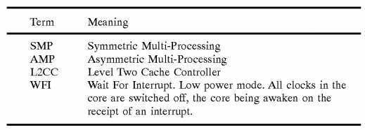
Terms and Abbreviations
This document uses the following terms and abbreviations.
We describe hereafter a global Multi-processing platform. The specified architecture should allow both?SMP?and AMP within the same platform, with the same programmer‘s model.
A typical MP system includes:
This architecture enables the development of Low?Power?Multi-processing systems (the WFI state for Low?Power?mode is supported).
This architecture should scale to cores having a private Level 2 cache.
Ease of integration of this architecture into already existent designs has been considered. The current specification should allow replacing a single core with an?SMP-capable system with no other change in the design.
Coherent Multiprocessing Memory System
The chosen solution is shown in?FIG. 1:
Two main tasks were identified to produce a multi-processing memory system:
Standard ARM cores should be modified to take advantage of the Multi-Processing environment:
However, an important point is that an?SMP?capable core will still be compatible with the standard AHB bus, and can work seamlessly in a non-Multiprocessing memory environment.
In the ARM MP-architecture, a centralized unit (dubbed the SCU, for Snoop Control Unit) controls AHB requests coming from the cores and checks them for coherency needs. This unit ensures that memory consistency is maintained between all caches. When necessary it sends control messages to data caches (INVALIDATE, CLEAN or COPY commands) and redirects memory transfers (directly between processors, or to the external AHB interface).
Different features can be added to the SCU. These features are mostly transparent to the programmer, and can improve performance and/or?power?consumption. These may be configurable, and can be arranged to ensure that their default configuration does not change the programmer‘s model. Although this is not mandatory, the SCU can for example maintain a local copy of all processors DATA TAG arrays to speed-up coherency lookups without having to ask (and therefore stall) processors in the memory system.
The SCU also uses an external master AHB interface. This interface can send writes requests to memory, and read data from the main memory if the requested line is not present in other Data caches (snoop miss). In order to ease the implementation of a?SMP-capable system, this external interface is designed to plug easily to a L2CC, an AMBA3 wrapper or a standard AHB bus.
At the SCU level, each memory request coming from an?SMP?core generates a coherency check. Only data-side caches of processors in the?SMP?memory system are looked up for the required data.
The cache coherency protocol used for the Core-SCU communication is based on the MESI protocol. However, it has been modified using a Berkeley approach to improve its performance and?power?consumption.
In a Multiprocessing memory system, the consistency model is an important piece of the Programmer‘s model. It defines how the programmer should expect the memory content to change while issuing reads and writes. The consistency model of the ARM MP architecture is the Weak Ordering model, which ensures correct program behaviour using synchronisation operations.
A bus between the core and the SCU, dubbed the Coherency Control Bus (CCB), is responsible for passing messages between the SCU and the cores. This defines a standard interface between a?SMP?capable core and the SCU.
As the?SMP?architecture evolves this allows the?SMP-core interface to remain stable.
This bus is also providing status signals mandatory to implement Multiprocessing features, as described in the Supported Features section given below.
In a multiprocessor system, one could imagine dedicating one or more processor(s) to non-SMP?tasks/OS. This means that this (these) processor(s) will never handle shared data.
This can be the case if someone wants to avoid porting applications from one OS to a new one. The solution is to run a separate OS on a dedicated processor, even if this OS is not?SMP?capable. This can also be considered for specific tasks/threads that do not need any OS support, like for example when running a dedicated multimedia task on a separate processor (which may have a specific or private coprocessor).
Processing coherency checks on each AHB request from these processors is useless, since they will never share data, and it penalises the performances of both the whole system (since you will add load to the SCU) and the processor itself (since you introduce latency on the AHB request for looking for coherency needs).
An attribute in CP?15?defines whether the processor is working in symmetrical mode or not. It defines if AHB requests from the processor should be taken into account by the SCU and whether this processor‘s Data cache has to be looked at upon coherency requests from other processors.
This attribute is sent to the SCU as a SCSMPnAMP bit.
When a processor requires a line which is stored in another processor‘s cache, the SCU can transmit the line from the processor having it to the one requesting it.
The goal is to limit accesses to the following memory level, those accesses penalising both timing and?power?consumption. The SCU will hence get the line from the owner, and will forward it to the requiring processor.
Different line status changes are defined, depending on the state of the line in the owning processor (Modified, Shared or Exclusive), the type of request (read or write) and whether the migratory line feature is enabled or not.
Coherency with Core OFF and Caches ON
An additional Wait-for-Interrupt instruction has been defined that allows turning off the core while maintaining coherency in the L1 caches (caches ON).
MP-capable cores thus have two Wait-for-interrupt instructions:
Both WFI instructions are implemented as CP?15?instructions.
The way the low-power?state is achieved is through clock-gating. A module at the CPU level stops the clock of the core or the clock of both the core and the cache.
The core escapes the low-power?WFI state upon reception of an interrupt.
The Coherency Control Bus (CCB) is responsible for passing coherency messages between an ARM MP-capable core and the Snoop Controller Unit (SCU).
This bus is originally designed for a multi-processing system based on the ARM1026 core family. The AMBA bus used between the ARM1026 core and the SCU is a private one.
However, the defined CCB specification is also applicable to the following memory environments:
The bullet specification of this Coherent Control Bus (CCB) is:
In the following chapter, we present the CCB scheme with more details in an AHB 2.0 memory environment.
When sending a memory request on the AMBA bus, a Multi-Processing?aware?core sets the "CCB core sideband" signals to indicate what type of memory burst is needed.
The value of this sideband bus distinguishes between the following operations:
A precise list of signals with their encoding is available below.
While ensuring the memory system consistency, the SCU may have to send coherency commands to all cores in the memory system.
The following coherency operations are defined:
Together with the coherency operation, a MESI state is sent. It indicates the final state of the cache line once the coherency operation has been processed.
The Snoop Controller Unit uses a private communication channel to send coherency commands to the core:
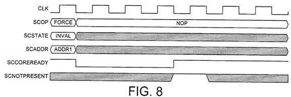
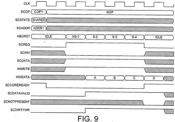
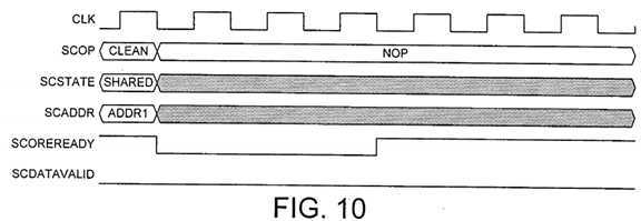
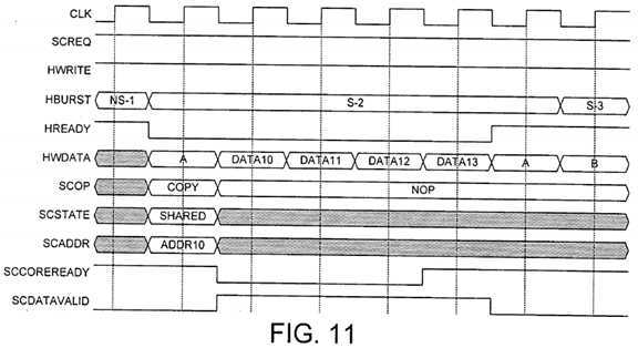
This bus does not depend on the AMBA bus. If a coherency request is required by the SCU while the SCCOREREADY signal is asserted, the core has to register the coherency request and drop the SCCOREREADY signal.
The SCCOREREADY signal should remain LOW as long as the core has not completed the coherency operation.
Please refer to timing diagrams and description below for more information regarding coherency requests management.
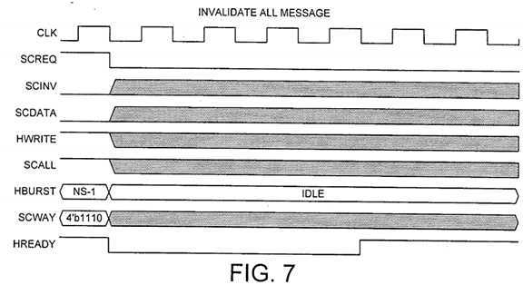
When a core issues a "CP15 INVALIDATE" or "CP15 INVALIDATE ALL" command on its data cache, it has to send a message to the SCU unit. This message is needed to force the SCU to update its Dual Tag arrays.
This "CP?15?notification" message is sent by the core as a single AHB WRITE cycle as follows (see timing diagrams):
This means that the AMBA address decoding logic (if any) sitting between the core and the SCU should always select the SCU slave port when receiving a memory request which has the SCREQ bit asserted.
Processing coherency requests at the core level
When the core receives a coherency command coming from the SCU on the SCOP bus, it registers the requested operation and is getting prepared to service the request.
Many cases may appear at the core interface:
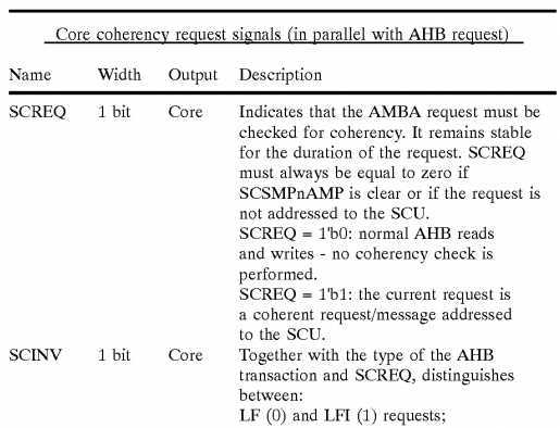
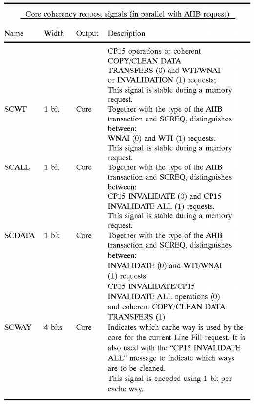
The Coherency Control Bus (CCB) can be divided in 4 signal groups:
SCU command signals: these signals are used by the SCU to send coherency commands to the core.
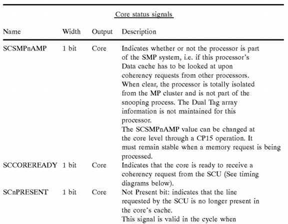

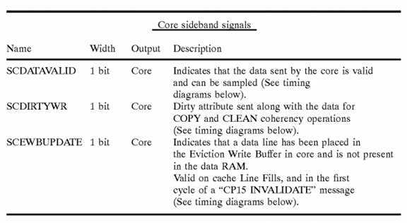
?
?
?
?
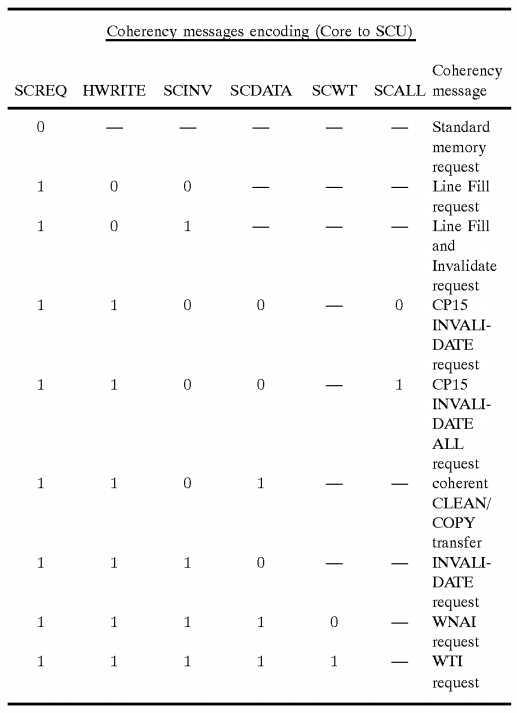
AHB2.0 Timing Diagrams
The following timing diagrams explain the core/SCU communication:
(See?FIG. 6)
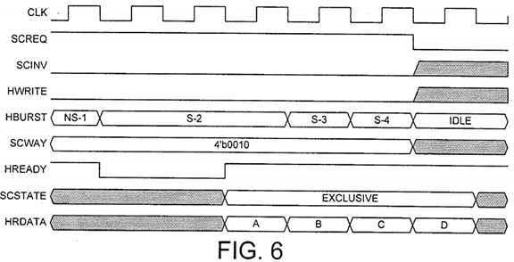
INVALIDATE All Message
(See?FIG. 7)
FORCE Command (not Present Case)
(See?FIG. 8)
COPY Command (Hit Case)
(See?FIG. 9)
CLEAN Command (Miss Case)
(See?FIG. 10)
Coherent Write Burst Delayed by a COPY Command
(See?FIG. 11)
Although illustrative embodiments of the invention have been described in detail herein with reference to the accompanying drawings, it is to be understood that the invention is not limited to those precise embodiments, and that various changes and modifications can be effected therein by one skilled in the art without departing from the scope and spirit of the invention as defined by the appended claims.
SRC=https://www.google.com.hk/patents/US20050005073
Power control within a coherent multi-processing system,布布扣,bubuko.com
Power control within a coherent multi-processing system
标签:des style blog http color os io strong
原文地址:http://www.cnblogs.com/coryxie/p/3926653.html