标签:stream into tween tab har set pix switch reduce
General Description
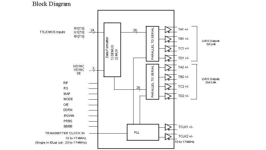
The THC63LVD827 transmitter is designed to supportpixel data transmission between Host and Flat PanelDisplay and Dual Link transmission between Host andFlat Panel Display up to 1080p/1920x1440 resolutions.
The THC63LVD827 converts 27bits (RGB 8 bits +Hsync, Vsync, DE) of CMOS/TTL data into LVDS(Low Voltage Differential Signaling) data stream. Thetransmitter can be programmed for rising edge or fallingedge clocks through a dedicated pin. For dual LVDS out, LVDS clock frequency of87MHz, 51bits of RGB data are transmitted at an effec-tive rate of 609Mbps per LVDS channel.
For single LVDS out, LVDS clock frequency of174MHz, 27bits of RGB data are transmitted at aneffective rate of 1218Mbps per LVDS channel.
21bits (RGB 6 bits + Hsync, Vsync, DE) mode is alsoselectable for 6bit color transmission with lower power.
Features
?Low power 1.8V CMOS design
?7mm x 7mm/72pin/0.65mm pitch/TFBGA package applicable to non-HDI PCB.
? Wide dot clock range, 10-174MHz, suited forTV Signal: up to 1080p(74.25MHz dual) PC Signal: up to 1920x1440(86MHz dual)
?Supports 1.8V single power supply
?1.8V/2.5V/3.3V TTL/CMOS inputs are supported by setting IOVCC=1.8V/2.5V/3.3V
?LVDS swing reducible by RS-pin to reduce both EMI and power consumption
? PLL requires No external components
?Flexible Input/Output mode
1. Single in / Dual LVDS out
2. Single in / Single LVDS out
3. Double edge Single in / Dual LVDS out
?2 LVDS data mapping to simplify PCB layout
?Power down mode
?Input clock triggering edge selectable by R/F pin
? 6bit / 8bit modes selectable by 6B/8B pinTHC
Pin Out (top view)
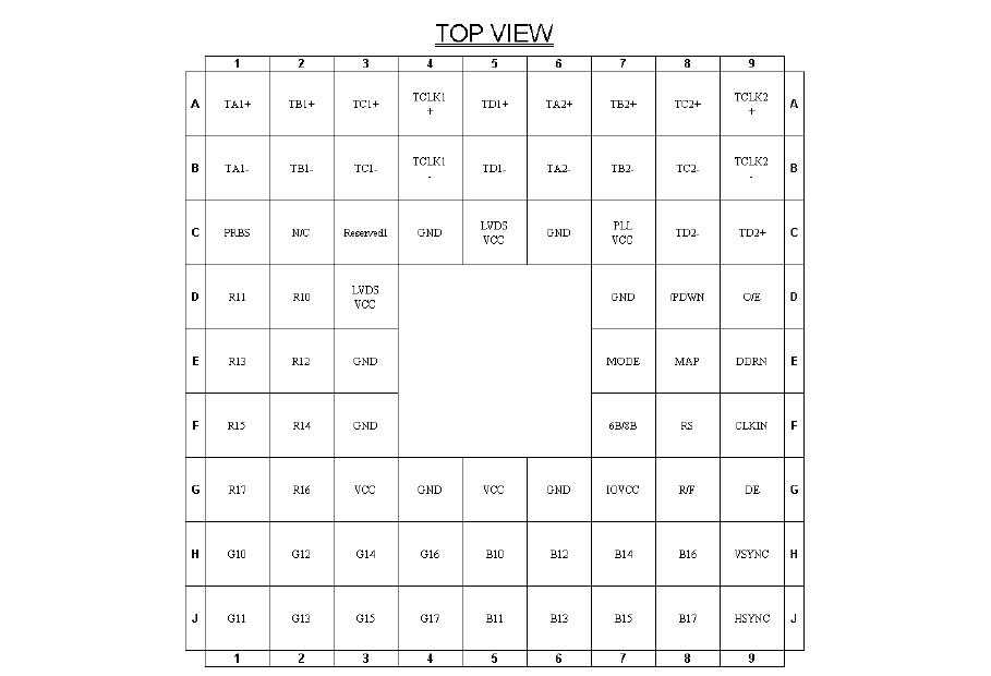
Pin Description
...
Absolute Maximum Ratings
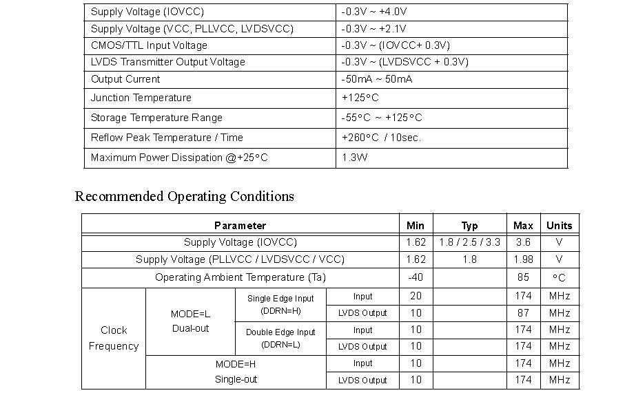
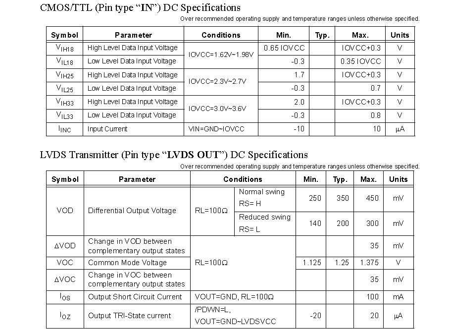
Electrical Characteristics
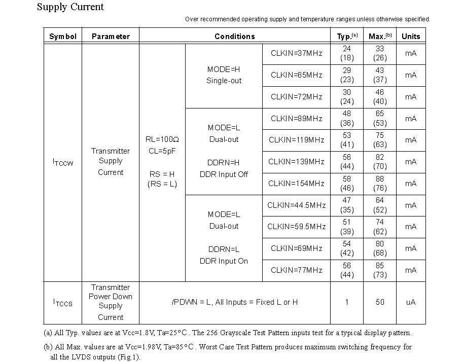

Switching Characteristics
...
AC Timing Diagrams
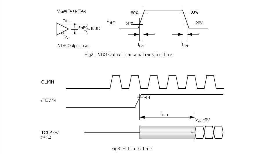
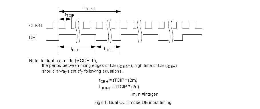
...
标签:stream into tween tab har set pix switch reduce
原文地址:http://www.cnblogs.com/TEL18218088355/p/7110263.html