标签:des blog http color ar 文件 2014 art sp
一.在原理图设计中,只要填footprint栏的信息即可,但在PCB editor中放置的时候找不到封装,路径的设置是在PCB editor中进行的
(1)先检查一下设计的封装文件是否齐全:dra、psm、pad、txt
(2)路径中不能有中文
(3)封装库的路径是否设定正确: setup->user preferences->design_paths中padpath和psmpath指到封装文件所在目录 setup->user preferences->config_paths中devpath指到封装文件所在目录
二.
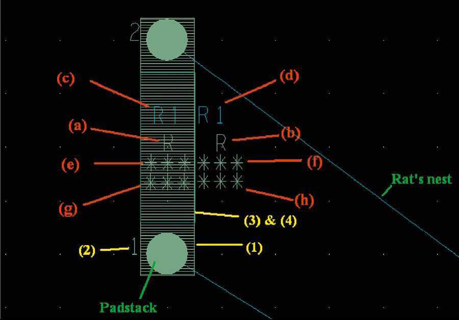
Text:
a. Assembly top (Comp Value)
b. Silkscreen top (Comp Value)
c. Assembly Top (Ref Des)
d. Silkscreen top (Ref Des)
e. Assembly top (Tolerance)
f. Silkscreen top (Tolerance)
g. Assembly top (User Part)
h. Silkscreen top (User Part)
Objects:
1. Place_Bound_Top (Package Geometry)
2. Pin_Number (Package Geometry)
3. Assembly_Top (Package Geometry)
4. Silkscreen_Top (Package Geometry)
控制其显示在:Display → Color/Visibility →Components
标签:des blog http color ar 文件 2014 art sp
原文地址:http://www.cnblogs.com/zhangxiujun/p/3969272.html