标签:des style blog http color io os ar strong
An embodiment provides a?virtual?address?cache?memory including: a TLB virtual?page memory configured to, when a rewrite to a TLB occurs, rewrite entry data; a data memory configured to hold?cache?data using a?virtual?page tag?or a page offset as a?cache?index; a?cache?state memory configured to hold a?cache?state for the?cache?data stored in the data memory, in association with the?cache?index; a first?physical?address memory configured to, when the rewrite to the TLB occurs, rewrite a held?physical?address; and a second physical?address memory configured to, when the?cache?data is written to the data memory after the occurrence of the rewrite to the TLB, rewrite a held physical?address.
An embodiment herein relates generally to a?virtual?address?cache?memory, a processor and a multiprocessor.
Conventionally, a processor employing?virtual?storage includes a TLB (translation lookaside buffer), which is a?cache?memory dedicated to holding a copy of a page table managed in an operating system (hereinafter referred to as "OS") in order to perform high-speed address translation from a?virtual?address space, which is an address space unique to a process, to a real address space, which is an address space of the entire computer system including the processor.
Meanwhile, in order to hide memory access latency, a processor copies data in a memory to a?cache?memory (hereinafter also referred to as "cache") to use the data. In order to identify the address of data in the memory, a copy of which has been hold in the?cache, in addition to a data memory configured to hold data in the memory, the processor includes a?tag?memory configured to store the addresses of the data and the states of the data (e.g., whether or not the data is valid, and whether or not the memory content has been updated). In general, a?tag?memory is configured to use low-order bits of a memory address as an?index?for a?cache, and hold high-order bits (tag) of the memory address and the state of data as data.
The aforementioned address translation is often a critical path for timing in processor designing. Where a processor employs hierarchical memories, a configuration in which a level 1?cache?positioned close to the processor (hereinafter referred to as "L1?cache") is accessed using a?virtual?address, and caches of level 2 ("L2?cache") onward are accessed using a?physical?address for, e.g., a countermeasure for aliases, which will be described later, is often employed.
Since address translation is performed in all of memory accesses for instruction fetching, load instructions and store instructions, the effect of TLB misses imposed on the performance is larger than that of ordinary?cache?misses. Accordingly, a TLB is provided as a dedicated memory separately from a?cache.
However, the configurations of the aforementioned conventional TLB and?cache memory have the following problem.
The problem is one relating to the capacities of?tag?memories in a TLB and a cache.
A TLB holds data such as?virtual?page numbers and?physical?page numbers, and page attributes and page states as its data. A processor having a?physicaladdress size of 32 bits or more has a large percentage of?virtual?page numbers and?physical?page numbers in the data held by the TLB. The size of a TLB is determined mainly by the size of the?physical address space, the minimum page size, and the number of entries in the TLB.
A?tag?memory of a?cache?holds data such as tags and the?cache?states as its data. A processor having a?physical?address size of 32 bits or more has a large percentage of tags in the data held by the?tag?memory of the?cache. The size of a?tag memory of a?cache?is determined mainly by the size of the?physical?address space, the?cache?line size, and the?cache capacity.
According to Figure 5.28 (p. 341) in "Computer Architecture—A Quantitative Approach—Fourth Edition", in a recent processor,
an L1?cache?is a 2-way set associative?cache?with a size of 8 to 64 KB.
a TLB is a full associative?cache?with an entry count of 40 to 1024; and
the minimum page size is 4 to 64 KB.
See also "Integrating?Virtual?Memory, TLBs, and Caches" (pp. 524-527), Figure 7.24 (p. 525), and Figure 7.25 (p. 526) by David A. Patterson and John L. Hennessy, Computer Organization and Design—The Hardware/Software Interface—Third Edition, Morgan Kaufmann Publishers, 2007, and "Avoiding address translation during indexing of the?cache?to reduce hit time" (p. 291) and Figure 5.3 (p. 292) by John L. Hennessy and David A. Patterson, Computer Architecture—A Quantitative Approach—Fourth Edition, Morgan Kaufmann Publishers, 2007.
(First Problem)
Conventionally, when task switching in which an executed task is switched to another occurs, the content of the TLB is rewritten, and processing for invalidating the?cache?memory is performed. Here, when data in the?cache?memory has been updated and a dirty bit is set, a write-back of?cache?data to the main memory is performed.
However, the time required for a write-back of data to the main memory is extremely long compared to time required for other processing in task switching, causing a problem in that the responsiveness of task switching in the processor deteriorates.
(Second Problem)
Furthermore, conventionally, a multiprocessor system includes a system in which data reads and writes are performed between the main memory and a?cache?memory in a processor, and between respective?cache?memories.
For example, in a multiprocessor system, when a processor writes an operation result to its own?cache?memory, the value of the data in the main memory corresponding to the operation result data differs from the data in the?cache?memory. Accordingly, when another processor refers to the operation result data, a write-back, that is, castout of the value written to the?cache?memory by the processor from the?cache?memory to the main memory is performed. As a result of the write-back being performed, correct data is stored in the main memory, enabling the operation result data to be used by another processor as well. In other words, in a multiprocessor system, in order to make data rewritten by a processor (CPU1) available to another processor (CPU2), the processor that has rewritten the data (CPU1) needs to write the data back to the main memory.
The aforementioned write-back involves access to the main memory, which results in the problems of causing a decrease in performance of the multiprocessor system due to large latency, and furthermore, causing an increase in power consumption due to an operation of the input/output circuit.
(Third Problem)
Furthermore, conventionally, DMA technique is used for data transfer between different address areas of a main memory or between the main memory and an input/output device without increasing the load of the CPU. For multiprocessor systems, a technique in which each processor performs data transfer between a main memory and its own local memory using DMA has been in practical use.
For example, a CPU of each processor, that is, a CPU core in a multiprocessor system accesses a relevant local memory according to a load instruction and a store instruction, reads data from the local memory according to the load instruction and writes the data to a register file in the CPU, and retrieves data from the register file in the CPU according to the store instruction and writes the data to the local memory. Each CPU performs a read (GET) of data to the local memory from the main memory and a write (PUT) of data from the local memory to the main memory using DMA.
DMA transfer is controlled by a DMA controller by means of designating a source address and a destination address, which are?physical?addresses. Furthermore, for the aforementioned multiprocessor system, DMA transfer of a cacheable area is not supported.
Accordingly, since a source address and a destination address are also designated using?physical?addresses in DMA, a programmer can write programs to be executed in the respective CPUs after estimating the data processing time and the data access time.
In order to increase the processing power of a processor in each CPU, a?cache?memory can be provided in the processor; however, accessing a main memory via a?cache?memory causes problems in that data access time differs between the case of a?cache?hit and the case of a?cache?miss, and the time required for transfer of?cache?data from the main memory in the case of a?cache?miss cannot be estimated.
Furthermore, in order to enhance the flexibility of program development, programs that can be executed in the aforementioned multiprocessor system can be made to be executable by using?virtual?addresses, which, however, causes a problem in that DMA cannot be used for a system using?virtual?addresses in a local memory.
(Fourth Problem)
In general,?cache?memories include multilevel?cache?memories, and some processors include multilevel caches. In that case, the storage capacity of an L1?cache?is smaller than the storage capacity of an L2?cache. In general, the storage capacity of a higher-order?cache?is smaller than the storage capacity of a lower-order?cache.
However, the hit rate of an L1?cache?is generally high. When an L1?cache?is accessed, a TLB is always referred to for translation from a?virtual?address to a?physical?address. Accordingly, a processor suffers large power consumption in the TLB hardware.
A present embodiment has been provided in view of the aforementioned first problem, and a first object of the present embodiment is to provide a?cache?memory and a processor, which provide a TLB function in the?cache?memory, enabling reduction of the circuit amount, and have enhanced task switching responsiveness.
Another present embodiment has been provided in view of the aforementioned second problem, and a second object of the present embodiment is to provide a multiprocessor system enabling reduction of the amount of access to a main memory based on data write-back processing performed by each processor.
A still another present embodiment has been provided in view of the third problem, and a third object of the present embodiment is to provide a processor enabling DMA to be executed using a?virtual?address, enhancing the?cache?hit rate for DMA transfer, or enhancing the?cache?hit rate for the case where the relevant processor accesses the?cache?after DMA transfer.
A still further present embodiment has been provided in view of the aforementioned fourth problem, and a forth object of the present embodiment is to provide a processor including multilevel?cache?memories, the processor enabling the reference frequency of a TLB to be reduced, decreasing the power consumption of the processor.
FIG. 1?is a configuration diagram illustrating a configuration of a processor system according to a present embodiment;
FIG. 2?is a configuration diagram of a?cache?memory according to a present embodiment, which is a?virtual?address?cachememory;
FIG. 3?is a flowchart illustrating processing for a memory read according to a present embodiment;
FIG. 4?is a flowchart illustrating TLB registration processing according to a present embodiment;
FIG. 5?is a flowchart illustrating TLB miss processing according to a present embodiment;
FIG. 6?is a flowchart illustrating processing for a?cache?read according to a present embodiment;
FIG. 7?is a flowchart illustrating processing for a memory write according to a present embodiment;
FIG. 8?is a flowchart illustrating processing for a?cache?write according to a present embodiment;
FIG. 9?is a configuration diagram of a?cache?memory including a configuration that reduces overhead for task switching according to a present embodiment;
FIG. 10?is a flowchart illustrating TLB rewrite processing according to a present embodiment;
FIG. 11?is a flowchart illustrating processing for a memory read where a configuration that reduces overhead for task switching is employed, according to a present embodiment;
FIG. 12?is a block diagram illustrating a configuration of a multiprocessor system?1A including a plurality of processors according to a present embodiment;
FIG. 13?is a flowchart illustrating processing upon occurrence of a?cache?miss in a processor, according to a present embodiment;
FIG. 14?is a flowchart illustrating an example of write-back processing upon occurrence of a?cache?miss, according to a present embodiment;
FIG. 15?is a flowchart illustrating processing performed by a memory controller?15?for a write-back, according to a present embodiment;
FIG. 16?is a diagram illustrating a manner of data write-backs according to a present embodiment;
FIG. 17?is a block diagram illustrating a configuration of a multiprocessor system?1B including a plurality of processors, according to a present embodiment;
FIG. 18?is a configuration diagram of a?cache?memory including a function that performs DMA transfer according to a present embodiment;
FIG. 19?is a flowchart illustrating processing in a GET operation using DMA, according to a present embodiment;
FIG. 20?is a flowchart illustrating processing in a PUT operation using DMA, according to a present embodiment;
FIG. 21?is a flowchart illustrating processing in a GET operation for a prefetch, according to a present embodiment;
FIG. 22?is a flowchart illustrating processing in a memory read 2 in S422?of?FIG. 21;
FIG. 23?is a flowchart illustrating processing in a?cache?read 2 in S431?of?FIG. 22;
FIG. 24?is a flowchart illustrating TLB registration processing including DMA processing, according to a present embodiment;
FIG. 25?is a flowchart illustrating?cache?read processing including DMA processing, according to a present embodiment;
FIG. 26?is a flowchart illustrating?cache?write processing including DMA processing, according to a present embodiment;
FIG. 27?is a block diagram illustrating a configuration of a multiprocessor system?1C including a processor including multilevel?cache?memories, according to a present embodiment;
FIG. 28?is a configuration diagram of an L2?cache?52?according to a present embodiment;
FIG. 29?is a configuration diagram illustrating a?cache?memory according to variation 3 of an L2?cache?52?according to a present embodiment;
FIG. 30?is a flowchart of a shared memory read in variation 3 of an L2?cache?52?according to a present embodiment;
FIG. 31?is a flowchart of a shared memory write in variation 3 of an L2?cache?52?according to a present embodiment;
FIG. 32?is a flowchart of TLB miss processing in variation 3 of an L2?cache?52?according to a present embodiment;
FIG. 33?is a flowchart of TLB registration processing in variation 3 of an L2?cache?52?according to a present embodiment;
FIG. 34?is a configuration diagram of a?cache?memory according to variation 4 of an L2?cache?52?according to a present embodiment; and
FIG. 35?is a configuration diagram of a?cache?memory according to variation 5 of an L2?cache?52?according to a present embodiment.
An embodiment enables provision of a?virtual?address?cache?memory including: a TLB?virtual?page memory configured to hold entry data including a?virtual?page?tag, the?virtual?page?tag?being a predetermined high-order bit (MSB side) of a virtual?address for a process, output a hit signal when the?virtual?page?tag?corresponds to a?virtual?page?tag?from a processor, and when a rewrite to a TLB occurs, rewrite the entry data; a data memory configured to hold?cache?data using the?virtual?page?tag?or a page offset as a?cache?index; a?cache?state memory configured to hold a?cache?state for the cache?data stored in the data memory, in association with the?cache?index; a first?physical?address memory configured to hold a?physical?address corresponding to the?virtual?address held in the TLB?virtual?page memory, and when the rewrite to the TLB occurs, rewrite the held?physical?address; and a second?physical?address memory configured to hold a?physical address for the?cache?data held in the data memory, and when the?cache?data is written to the data memory after the occurrence of the rewrite of the TLB, rewrite the held?physical?address.
An embodiment enables provision of a processor including: processors connected via a bus, each processor including a CPU, a?cache?memory and a DMA controller; and a memory controller connected to the bus, the memory controller being a control section for a main memory, wherein the?cache?memory includes: a TLB?virtual?page memory configured to hold entry data including a?virtual?page?tag, the?virtual?page?tag?being a predetermined high-order bit (MSB side) of a?virtual address for a process, output a hit signal when the?virtual?page?tag?corresponds to a?virtual?page?tag?from a processor, and when a TLB miss occurs, rewrite the entry data; a data memory configured to hold?cache?data using the?virtual?page tag?or a page offset as a?cache?index; a?cache?state memory configured to hold a?cache?state for the?cache?data stored in the data memory, in association with the?cache?index; a first?physical?address memory configured to hold a?physical address corresponding to the?virtual?address held in the TLB?virtual?page memory, and when the TLB miss occurs, rewrite the held?physical?address; and a second?physical?address memory configured to hold a?physical?address for the?cache data held in the data memory, and when the TLB miss occurs, rewrite the held?physical?address, and wherein when data is transferred by DMA transfer using the DMA controller from the main memory to the?cache?memory, the CPU sets a transfer source address and a transfer destination address in the DMA transfer, using?virtual?addresses.
An embodiment enables provision of a processor including: a CPU; a primary?cache?memory; and a secondary, or tertiary or more-order?cache?memory, wherein the secondary or tertiary or more-order?cache?memory includes: a TLB?virtual?page memory configured to hold entry data including a?virtual?page?tag, the?virtual?page?tag?being a predetermined high-order bit (MSB side) of a?virtual?address for a process, and output a hit signal when the?virtual?page?tag?corresponds to a?virtualpage?tag?from a processor; a data memory configured to hold?cache?data using the?virtual?page?tag?or a page offset as acache?index; and a?cache?state memory configured to hold a?cache?state for the?cache?data stored in the data memory, in association with the?cache?index.
Hereinafter, embodiments will be described with reference to the drawings.
(Configuration)
First, a processor system according to a present embodiment will be described with reference to?FIG. 1.?FIG. 1?is a configuration diagram illustrating a configuration of a processor system according to a present embodiment.

A processor system?1?includes a central processing unit (hereinafter referred to as "CPU")?11, a level 1 (L1)?cache?memory12, which is a?virtual?address?cache?memory, and one or more DRAMs?13?(hereinafter, only referred to as DRAM?13), which is a main memory. The processor system?1?is a processor including a?virtual?storage mechanism and a?cache memory. The CPU?11?is what is called a CPU core. The?cache?memory?12?includes a?cache?memory control circuit. The cache?memory?12?and the DRAM?13?are interconnected via a bus. The DRAM?13?is connected to the bus via a memory controller (not illustrated). Here, although the main memory is described taking a DRAM as an example, the main memory may be another type of memory.
Although the present embodiment is described in terms of an example in which one CPU?11?accesses the DRAM?13, a multicore configuration may be used in which a plurality of CPU?11-cache?memory?12?pairs, and the plurality of pairs are connected to one DRAM?13?via, e.g., a system bus. Also, the DRAM may be separated into a plurality of memories according to addresses, and may include a memory other than a DRAM, for example, an SRAM.
Furthermore, e.g., an L2?cache?may be provided between the?cache?memory?12, which is an L1?cache, and the DRAM?13.
The CPU?11?reads an instruction or data stored in the main memory?13?via the?cache?memory?12?to execute a program. If an instruction or data (hereinafter also simply referred to as "data") necessary to execute a program exists in the?cache memory?12, the CPU?11?reads the instruction or data to execute the program.
In order to designate the data, the CPU?11?outputs a?virtual?address EA to the?cache?memory?12. If data corresponding to the input?virtual?address exists in the?cache?memory?12, the?cache?memory?12?outputs the data to the CPU?11. If no such data stored in the?cache?memory?12, the data is read from the DRAM?13?by means of refilling, written to the?cache?memory12, and then output to the CPU core?11.
In the?cache?memory?12?according to the present embodiment,?cache?entry replacement is performed on a?virtual?page basis managed by an OS managing the execution of a plurality of processes, and?cache?state management is performed on a?cache?line basis, that is, on a?cache?block basis. In the processor system according to the present embodiment, thecache?memory?12?is accessed using a?virtual?address, and the?cache?coherency is maintained by means of snooping. For snooping, see "5.1.2.?Cache?Coherence through Bus Snooping" (p. 277), Figure 5.4 (p. 278), "6.2. Base Design: Single-level Caches with an Atomic Bus" (pp. 380-393), Figure 6.4 (p. 386) and Figure 6.5 (p. 388) by David E. Culler, Jaswinder P. Singh and Anoop Gupta, Parallel Computer Architecture—A Hardware/Software Approach—, Morgan Kaufmann, 1999, ISBN 1-55860-343-3.
FIG. 2?is a configuration diagram of the?cache?memory?12, which is a?virtual?address?cache?memory.

The?cache?memory?12?includes a TLB?virtual?page memory (TLB EP memory)?21, a TLB?physical?page memory (TLB RP memory: first?physical?address memory)?22, a data memory?23, a?cache?state memory?24, and a TLB?physical?page CAM memory (TLB RP CAM memory: second?physical?address memory)?25.
The?cache?memory?12?receives an input of a?virtual?address (EA) from the CPU?11?and outputs a?physical?address?32?to the DRAM?13.
The?cache?memory?12?provides functions as a TLB and an L1?cache?by means of a?cache?memory with 4-way set associative configuration. The capacity of the?cache?memory?12?as an L1?cache?is 256 KB (kilo bytes; the same applies to the description below).
Although the size of each way exceeds the page size, no "page coloring which will be described later", has been performed for the?virtual?addresses.
The?cache?memory?12?is a 4-way set associative?cache?in which?virtual?addresses EA are divided in units of page of 4 KB, and constitutes a TLB and an L1?cache. In the present embodiment, for example, the?cache?memory?12?as an L1?cache?is accessed by a 32-bit?virtual?address?31.
High-order bits (31:12) in the?virtual?address EA form a?virtual?page?tag?(EP_Tag), and middle-order bits (15:12) indicating a space obtained as a result of 64 KB, which is a?cache?capacity per way, being divided by 4 KB, forms a?virtual?page index?(EP_index; hereinafter also referred to as "TLB?index"). Furthermore, bits (11:7) form a page offset, bits (6:2) form a block offset, and a lowest-order bit (1:0) forms a word offset.
Since the size of each way (64 KB) is larger than the page size (4 KB), as illustrated in?FIG. 2, the bits (31:12) and (15:12) of the?virtual?address EA are allocated to the?virtual?page?tag?and the?virtual?page?index, respectively, which overlap each other.
From the CPU?11, a process number PID as an identifier for identifying a process is also input to the?cache?memory?12.
Then, the CPU?11?reads data of a size equal to or smaller than the?cache?line size from the?cache?memory?12. Here, the CPU?11?reads 32-bit data from the?cache?memory?12.
The TLB?virtual?page memory?21?includes TLB?virtual?page memories, each of which is attached to each way. Each TLBvirtual?page memory can store data such as state information indicating the state of each page, e.g., valid (V), reference (R) and dirty (D), a process number PID as an identifier for identifying a process, a?virtual?page number EP and a way number WN. The?virtual?page number EP is data corresponding to high-order bits (31:12) in a?virtual?address EA. In this example, same values as those of the way numbers of the TLB are used for way numbers WN, and thus, fields for the way numbers WN may be provided, or a configuration in which the fields for the way numbers WN are omitted using the way numbers of the TLB may be employed. It is supposed that a processor with an architecture not having process numbers performs an operation in the present embodiment using?virtual?page numbers only, not using process numbers.
Each data in the TLB?virtual?page memory?21?is designated by 4 bits (15:12) of a?virtual?address EA, which forms a TLBindex.
Four comparators?21?a?are provided. Each comparators?21?a?compares a process number PID and a?virtual?page number EP of each TLB?virtual?page memory?21, and a process number PID and a?virtual?page?tag?EP_Tag in a?virtual?address EA from the CPU?11. The four comparators?21?a?output a way number WN as a hit signal when there is a hit, and a non-hit signal when there is no hit, as an output of the TLB?virtual?page memory?21.
The TLB?physical?page memory?22?includes TLB?physical?page memories, each of which is attached to each way. Each data in each TLB?physical?page memory?22?is designated by a?virtual?page?index?EP_Index.
Data in the TLB?physical?page memory?22, that is,?physical?page numbers RP, are associated with both the respective ways of the TLB?virtual?page memory?21?and the?virtual?page indexes EP_Index, and a?virtual?address space is managed in units of 4 KB per page.
Data in the TLB?physical?page memory?22?are used in the case of a?cache?miss and a TLB miss. The TLB?physical?page memory?22?outputs four?physical?address page bits (39:12) for the respective ways.
The data memory?23?includes data memories, each of which is attached to each way. Each data memory?23?manages cache?data in units of, for example, 128 bytes. Data in each data memory?23?is designated by 9 bits (a?virtual?page?index and a page offset) (15:7) and a block offset (6:2) in a?virtual?address?31?as a?cache?index.
Replacement of?cache?data from the CPU?11, that is, loading or storage to the data memory?23?is performed in word size (units of 32 bits). Data replacement via a system bus is performed by?cache?line size.
An output of each data memory?23?is input to a relevant 32-input, 1-output multiplexer (32:1 MUX)?23?a. A plurality of the multiplexers?23?a?(here, four multiplexers?23?a), each of which is selector, are provided in association with the respective data memories. A multiplexer?23?a?selects and outputs?cache?data in a block selected by a block offset (6:2) from among the data selected by a?virtual?page?index?and a page offset.
A?cache?state memory (hereinafter also referred to as "state memory")?24?includes?cache?state memories, each of which is attached to each way. Data in each?cache?state memory?24?is designated by 9 bits (15:7) in a?virtual?address EA. The cache?state memory?24?is a memory for managing the state of the?cache?on a?cache?line basis (cache?block basis).
In order to allow multitasking, the?cache?state memory?24?stores data for the states of the?cache?blocks based on, for example, the MESI protocol. In the case of the MESI protocol, data in the M (Modified), E (Exclusive), S (Shared) and I (Invalid) states are stored. For the MESI protocol, see "5.3.2. A Four-State (MESI) Write-Back Invalidation Protocol" (p. 299), and Figure 5.15 (p. 301) by David E. Culler, Jaswinder P. Singh and Anoop Gupta, Parallel Computer Architecture—A Hardware/Software Approach—, Morgan Kaufmann, 1999, ISBN 1-55860-343-3, which is mentioned above.
Output data from the?cache?state memory?24?is data indicating the state of each data in the data memory?23, that is, data indicating, e.g., the validity/invalidity of the data, and the possibility/impossibility of a read. The output data is input to a control circuit (not illustrated) and used.
The TLB?physical?page CAM?25?includes TLB?physical?page CAMs (Content Addressable Memories), each of which is attached to each way. Data in each TLB?physical?page CAM includes a?physical?page number and valid state information.
The TLB?physical?page CAM?25?stores data for?physical?page numbers in association with the respective ways of the TLB virtual?page memory?21?and?virtual?page indexes. Data is registered in the TLB?physical?page CAM?25?when data is registered in the TLB?virtual?page memory?21.
The TLB?physical?page CAM?25?is used for a reverse search for a?virtual?page from a?physical?page and an alias check upon occurrence of a TLB miss in order to maintain the data coherency with another processor. Also, a?physical?page RP registered in the TLB?physical?page CAM?25?is the same as a?physical?page RP in the TLB?physical?page memory?22, which has an entry number corresponding to the?physical?page RP registered in the TLB?physical?page CAM?25. The access frequencies of the TLB?physical?page CAM?25?and the TLB?physical?page memory?22?are much lower than that of the TLB?virtual?page memory?21, and thus, the function of the TLB?physical?page memory?22?may be included in the TLB physical?page CAM?25.
The alias problem is a problem that when a?virtual?address is used for an L1?cache, which is larger than the page size, if a same?physical?address is allocated to another?virtual?address, data existing in the?cache?may be dealt with as data for a different address, causing data incoherency.
There have been two conventional methods for preventing this problem. In one method, upon occurrence of a TLB miss, all the entries that may cause an alias are checked, and if the?physical?addresses of entries correspond to each other, all the?cache?lines belonging to a relevant?virtual?page are flashed.
In the other method, a plurality of pages are arranged to create an address space using, for example, software that manages?virtual?addresses such as an OS (in the above example, 16 4-KB pages are arranged to create an area of 256 KB/4 ways=64 KB) to prevent occurrence of aliases by means of software, which is called page coloring.
However, in either case, when the same page is shared by a plurality of processes, it is necessary that simultaneously with replacement of a TLB entry as a result of occurrence of a TLB miss, data belonging to a page used in an old process be once totally invalidated in the?cache, and then reloaded using a new TLB entry.
In particular, in the alias problem, although programming is performed with the intension to share data between a plurality of processes, shared data is once invalidated in the?cache, and data that is entirely the same as the shared data is loaded to the?cache?using a new?virtual?address. Consequently, the relevant process and the entire system suffer deterioration in performance, resulting in a power consumption increase.
Also,?physical?addresses output to the bus connected to the DRAM?13?are monitored by means of what is called snooping, and input to the TLB?physical?page CAM?25. When a?physical?address having a same?physical?page number as that registered in the TLB?physical?page CAM?25?is detected from among the monitored, that is, input?physical?addresses, state data in the?cache?state memory?24?for a same entry number as that of the TLB?physical?page CAM?25?is changed. In other words, as a result of employing a?cache?coherency mechanism using snooping, the consistency of the state data in the cache?state memory?24, which indicate the states for all the?cache?lines having a same?physical?address, can be maintained. Also, when it is necessary to output data from the?cache?according to a coherence protocol, e.g., when the cache?have data newer than data recorded in the DRAM?13?as a result of snooping like in a "Modified" state according to the MESI protocol, data in the data memory?23?indicated by a same entry number as that in the TLB?physical?page CAM25?is accessed to output the data to the bus. As described above, the TLB?physical?page CAM?25?is used for processing for coherency maintenance.
Also, when a TLB miss occurs during execution of a plurality of processes, the aforementioned alias problem may occur, and thus, the TLB?physical?page CAM?25?is used when a TLB?physical?page memory miss occurs.
Outputs of the TLB?physical?page memory?22, the multiplexers?23?a?and the?cache?state memory?24?are input to respective 4-input, 1-output multiplexers (4:1 MUX)?22?b,?23?b?and?24?b. The respective multiplexers?22?b,?23?b?and?24?b, which are selectors, select and output data selected according to a way number from the TLB?virtual?page memory?21.
In the present embodiment, the CPU?11?is configured to retrieve data in a data width of 32 bits, but any data width that is equal to or smaller than the?cache?line size may be employed depending on the specifications of the processor core.
Next, operations of the?cache?memory?12?will be described. The description below is given in terms of a memory access request from the processor and a snoop response to the memory access request, which are equivalent to those according to a coherency control protocol used in a processor for a commercially-available multiprocessor, for example, the IBM PowerPC 970 FX RISC Microprocessor. For the IBM PowerPC 970 FX RISC Microprocessor, see IBM PowerPC 970 FX RISC Microprocessor User‘s Manual Version1.7 (which can be obtained as of Sep. 30, 2009 from the following URL: https://www-01.ibm.com/chips/techlib/techlib.nsf/products/PowerPC—970MP_Microprocessor) as a reference.
(Memory Read Operation)
FIG. 3?is a flowchart illustrating processing for a memory read.?FIG. 4?is a flowchart illustrating TLB registration processing. FIG. 5?is a flowchart illustrating TLB miss processing.?FIG. 6?is a flowchart illustrating processing for a?cache?read.

First, the overall processing in the processor system?1?will be described using?FIGS. 3 to 6.
As illustrated in?FIG. 3, when a memory read operation is started, the TLB?virtual?page memory?21, the data memory?23and the state memory?24?are accessed using a?virtual?index?(S1). If there is no hit in the TLB?virtual?page memory?21?(S2: NO), TLB registration processing for a read is executed (S3). If there is a TLB hit (S2: YES), whether or not the?virtual page is readable is determined (S4). If the?virtual?page is readable (S4: YES), a?cache?read is performed (S5). If the?virtual page is not readable (S4: NO), a notice of a protection violation is sent to a CPU?11?by means of interrupt processing (S6), and exception processing is performed by the OS.
As illustrated in?FIG. 4, when TLB registration processing is started, processing for reading a PTE (page table entry) to be registered is performed on the DRAM?13?(S11). Whether or not the PTE (page table entry) to be read exists in the DRAM13?is determined (S12). If the PTE does not exist (S12: NO), a notice of occurrence of an exception is sent to the OS (S13).

If the PTE exists (S12: YES), whether or not the cause of the TLB miss is a store instruction is determined (S14).
If the cause is not a store instruction (S14: NO), whether or not to permit this process to perform a read is determined (S23). If the process is not permitted to perform a read (S23: NO), the processing advances to S13. If the process is permitted to perform a read (S23: YES), a reference bit in the PTE is set (S24), and the processing advances to S17.
Then, whether or not the read PTE and any of all the valid TLB entries correspond to each other in terms of?physical?page number is determined (S17). If the?physical?page numbers do not correspond to each other (S17: NO), TLB miss processing is executed (S18), and a new PTE is registered as a TLB entry (S19).
On the other hand, if the?physical?page numbers correspond to each other (S17: YES), whether or not the corresponding TLB entry and the entry to be registered are the same in terms of?virtual?index?is determined (S20). If the?virtual?indexes are not the same (S20: NO),?cache?flash is performed for the page for the corresponding TLB entry (S21), and the processing advances to S18.
If the?virtual?indexes are the same (S20: YES), the?virtual?page number, the process number and the protection information of the TLB entry having the corresponding?physical?page number are rewritten (S22).
As illustrated in?FIG. 5, when TLB miss processing is started, whether or not an unused TLB entry exists in the same virtual?index?is determined (S31). If an unused TLB entry exists (S31: YES), the processing is ended.

If no unused TLB entry exists (S31: NO), a TLB entry to be evicted is determined (S32), and whether or not "Modified" cache?lines exist in the TLB entry to be evicted is determined (S33). If no "Modified"?cache?lines exist (S33: NO), the processing is ended.
If "Modified"?cache?lines exist (S33: YES), all the "Modified"?cache?lines that exist in the page to be evicted are flashed (S34), and the processing is ended.
As illustrated in?FIG. 6, when?cache?read processing is started, an output of the state memory?24?searched for using the virtual?index?is selected according to a?virtual?page offset and a block offset (S41), and a?cache?state output for the page having a TLB hit is selected (S42) and whether or not there is a?cache?hit is determined (S43). If there is no?cache?hit (S43: NO), a?physical?address is generated from the?physical?page number in the TLB to issue a memory access request (S44). This memory access request is similar to a request processed in a Read transaction or BusRd transaction in a PowerPC 970 FX processor. See the PowerPC 970 FX Read transaction section in IBM PowerPC 970 FX RISC Microprocessor User‘s Manual Version 1.7, which is mentioned above, and BusRd transaction in Figure 6.5 in Parallel Computer Architecture—A Hardware/Software Approach—, which is also mentioned above.

Then, the obtained data is loaded to the?cache?memory (S45).
The memory access request is snooped by the memory and other processors. Each of the processors that have snooped the memory access request checks the?cache?state managed by the processor itself, and if the?cache?state is "Modified", the processing returns a "Modified" response as a snoop response, and if the?cache?state is "Exclusive" or "Shared", returns a "Shared" response, and thus, the processor that has output the request updates the state data in the?cache?state memory?24?according to the snoop response. In other words, if the snoop response is a "Shared" response or a "Modified" response (S46: YES), the state of the request target?cache?line in the?cache?state memory?24?is changed to "Shared" (S47), and if the snoop response is neither a "Shared" response nor a "Modified" response (S46: NO), the state of the request target?cache?line is changed to "Exclusive" (S48). Then, the data is sent to the CPU?11?(S49).
If there is a?cache?hit (S43: YES), an output of the data memory searched for using the?virtual?index?is selected according to a way number from the TLB (S50), and the processing advances to S49. When there is a?cache?hit, no memory access request is issued, and the?cache?state is not updated.
(Memory Write Operation)
FIG. 7?is a flowchart illustrating processing for a memory write.?FIG. 8?is a flowchart illustrating processing for a?cache write.

As illustrated in?FIG. 7, when a memory write is started, the TLB?virtual?page memory?21, the data memory?23?and the state memory?24?are accessed using a?virtual?index?(S61). If there is no hit in the TLB?virtual?page memory?21?(S62: NO), TLB registration processing for a write is performed (S63). If there is a hit in the TLB (S62: YES), the case is determined as a case of a TLB hit, and whether or not the relevant?virtual?page is writable is determined (S64). If it is writable (S64: YES), a?cache?write is performed (S65). If it is not writable (S64: NO), a notice of a protection violation is sent to the CPU11?by means of interrupt processing (S66), and exception processing is performed by the OS.
As illustrated in?FIG. 4, when TLB registration processing is started, processing for reading a PTE to be registered is performed on the DRAM?13?(S11). Whether or not the PTE to be read exists in the DRAM?13?is determined (S12). If the PTE does not exist (S12: NO), a notice of occurrence of an exception is sent to the OS (S13).
If the PTE exists (S12: YES), whether or not the cause of the TLB miss is a store instruction is determined (S14). If the cause is a store instruction (S14: YES), whether or not to permit this process to perform a write is determined (S15). If the process is not permitted to perform a write (S15: NO), the processing advances to S13.
If the process is permitted to perform a write (S15: YES), a reference bit and a dirty bit in the PTE are set (S16).
Then, whether or not the read PTE and any of all the valid TLB entries correspond to each other in terms of?physical?page number is determined (S17). If the?physical?page numbers do not correspond to each other (S17: NO), TLB miss processing is executed (S18), a new PTE is registered as a TLB entry (S19).
On the other hand, if the?physical?page numbers correspond to each other (S17: YES), whether or not the corresponding TLB entry and the entry to be registered are the same in terms of?virtual?index?is determined (S20). If the?virtual?indexes are not the same (S20: NO),?cache?flash is performed for the page for the corresponding TLB entry (S21), and the processing advances to S18.
If the?virtual?indexes are the same (S20: YES), the?virtual?page number, the process number and the protection information of the TLB entry having the corresponding?physical?page number are rewritten (S22).
The TLB miss processing is similar to the above-described operation for a memory read.
As illustrated in?FIG. 8, when?cache?write processing is started, an output of the state memory?24?searched for using thevirtual?index?is selected according to a?virtual?page offset and a block offset (S71), and a?cache?state output for the page having a TLB hit is selected (S72).

Then, whether or not there is a?cache?hit is determined (S73). If there is no?cache?hit (S73: NO), a?physical?address is generated from the?physical?page number in the TLB to issue a memory access request (S74). In this case, the output memory access request is a "Memory read request for invalidating other?cache?lines", for example, RWITM or BUSRdx. The memory access request is snooped by the memory and other processors. A processor that has snooped the memory access request checks the?cache?state managed by the processor itself, and if the?cache?state is "Modified", the processor outputs a "Modified" response as a snoop response, and changes the?cache?state to "Invalid", and outputs data in the request target?cache?line to the requestor processor. Here, the memory cancels read access to the request target?cache line and data output to the requestor processor. If the?cache?state is "Exclusive" or "Shared", the processor returns a "Shared" response, and changes the?cache?state to "Invalid". The data in the request target?cache?line is output by the memory to the requestor processor. Then, the obtained data is loaded to the?cache?memory (S75), and the data received from the CPU?11?is written over the?cache?data. The processor that has output the request updates the state data in the cache?state memory?24?in response to the snoop response. Furthermore, the processor that has output the memory read request (RWTIM or BusRdX) updates the state of the request target?cache?line in the?cache?state memory?24?to "Modified" (S79).
If there is a?cache?hit (S73: YES), an output of a data memory searched for using a?virtual?index?is selected according to a way number from the TLB (S76), and the processing advances to S77. If the?cache?state is "Modified" (S77: YES), the cache?state is not changed. If the?cache?state is "Exclusive" (S78), the?cache?state is changed to "Modified" (S79). If the cache?state is "Shared" (S78: NO), the processor issues a?cache?line invalidation transaction (DClaim) (S80). Then, when the processor invalidates a?cache?in the other processors and receives a snoop response, the processor changes the cache?state to "Modified" (S79). When the?cache?state is changed to "Modified", the data from the processor is written to the?cache?(S81). This?cache?line invalidation transaction is similar to a request dealt with in a DClaim transaction in a PowerPC 970FX or a BusRdX transaction.
See PowerPC 970FX‘s DClaim transaction in IBM PowerPC 970FX RISC Microprocessor User‘s Manual Version 1.7, and BusRdX transaction in Parallel Computer Architecture—A Hardware/Software Approach—, which have been mentioned above as references.
Next, operations of the cases of a TLB hit and a TLB miss will be described with reference to?FIG. 2.
(Case of TLB Hit)
First, a?virtual?address EA and a process number PID are input from the CPU?11?to the?cache?memory?12. In the TLBvirtual?page memory?21, data in the respective ways are selected using a?virtual?page?index?(15:12) in the input?virtual address. Then, the input process number and a?virtual?page?tag?(31:12) in the input?virtual?address are compared respectively with a process number and a?virtual?page of each of the selected data in the TLB?virtual?page memory?21, and if the input process number and the?virtual?page?tag?correspond to a process number and a?virtual?page in the TLB?virtual page memory, the TLB?virtual?page memory?21?outputs a corresponding way number WN from a comparator?21?a?as a hit signal. If the input process number and the?virtual?page?tag?do not correspond to any process number and?virtual?page in the TLB?virtual?page memory, a non-hit signal indicating non-correspondence is output.
Here, each?virtual?page EP in the TLB?virtual?page memory?21?includes a?virtual?page?index?EP_Index because the?virtual page?index?EP_Index is used as a?virtual?tag.
The TLB?physical?page memory?22?selects a page number for a?physical?address using the?virtual?page?index?EP_Index (15:12) in the input?virtual?address. Except when a?cache?miss occurs or other caches are invalidated,?physical?page information held in the TLB?physical?page memory?22?is not used, and thus, an arrangement in which access to the TLBphysical?page memory?22?is started when information in the TLB?physical?page memory?22?become necessary may be provided.
In the data memory?23, data in a?cache?block is selected using 9 bits (15:7) and a block offset (6:2) in the 31-bit?virtual address. In other words, the multiplexers?23?a?select one data (32 bits) in one block, that is, one line (128 bytes) using the block offset (6:2) in the input?virtual?address. Accordingly, four?cache?block data are output from the four ways of the data memory?23, and four data (each having 32 bits) corresponding to the four ways are output from the multiplexers?23?a.
Also, the?cache?state memory?24?selects state data of?cache?blocks (cache?state data) in the respective ways using the 9 bits (15:7) in the?virtual?address and output the state data.
Accordingly, when there is memory read access to the DRAM?13?from the CPU?11?as a processor core, the following operation is performed.
First, the TLB?virtual?page memory?21?is accessed using a?virtual?page?index?EP_Index (15:12) in a?virtual?address as a TLB?index. In the TLB?virtual?page memory?21, an entry whose?virtual?address (31:16) and process number correspond to a process number and the?virtual?page?index?EP_Index (15:12) from the CPU?11?are searched for according to the TLBindex.
The TLB?virtual?page memory?21?outputs information of whether or not there is a way including the corresponding entry, and if there is, outputs a way number WN for the entry. If there is no corresponding entry, the access is dealt with as a TLB miss.
Hereinafter, the case where there is a corresponding entry will be described. Using bits (15:7) in the 31-bit?virtual?address as a?cache?index, the data memory?23, which is the L1?cache, is accessed. Then, a block offset (6:2) is input to the multiplexers?23?a?and data from the respective ways are output. In the configuration of the present embodiment, 32 bit-width data is delivered to the CPU?11, and thus, using the block offset (6:2), one 32 bit-width data is selected by the multiplexers?23?a?from the outputs of the respective ways.
Using a way number WN output from the TLB?virtual?page memory?21, only data in a way having a hit is selected by the multiplexer?23?b, which is a selector, and output.
Then, also using the way number WN output from the TLB?virtual?page memory?21, the state memory?24?selects and outputs data in the way having a hit only, by means of the multiplexer?24?b, which is a selector, (S42?in?FIG. 6) simultaneously with the output of the data from the data memory?23.
If the state output from the state memory?24?(cache?state) is a state other than "Invalid", the data output from the data memory?23, which is the L1?cache, can be used (S47) and thus, is output to the CPU?11?(S49). If the state (cache?state) is "Invalid", a?cache?miss processing operation will be performed (S44).
As described above, if there is a hit in both of the TLB and the?cache, the processing can be proceeded using a?virtualaddress EA only. In other words, if there is a hit in both of the TLB and the?cache, there is no need to use the TLB?physicalpage memory?22.
Next, the case of a?cache?miss will be described.
If a?cache?miss occurs when there is a TLB hit, the following operation is added. The case where a?cache?miss occurs when there is a TLB hit means the case where although there is a TLB hit, the?cache?state is "Invalid", requiring data for the?cache?to be read from the DRAM?13.
The TLB?physical?page memory?22?is accessed using a?virtual?page?index?EP_Index (15:12) in a?virtual?address as an index. Since the TLB?physical?page memory?22?is of a 4-way set associative type, the TLB?physical?page memory?22outputs four?physical?page numbers.
The multiplexer?22?b?selects one from the output?physical?page numbers using a way number WN from the TLB?virtual page memory?21.
Lower-order bits (11:0) in the?virtual?address, which is a target of a read request from the CPU?11?is combined with the selected?physical?page number (39:12) to generate a?physical?address RA (39:0), and the read request is sent to the DRAM?13?(S44). The obtained data is written to a relevant area in the data memory?23?(S45).
(Case of TLB Miss)
The following operation is added when there is a TLB miss.
A PTE for the relevant?virtual?page is loaded from the DRAM?13?(S11?in?FIG. 4). Then, the?physical?page number is input to the TLB?physical?page CAM?25, and whether or not a same?physical?page number as the?physical?page number exists is checked.
If there is no same?physical?page number, the following registration processing is performed (S17?onward). In other words, a?virtual?page number is obtained from the read PTE and data registration is performed for the TLB?virtual?page memory21, the TLB?physical?page memory?22?and the TLB?physical?page CAM?25?(S18?in?FIG. 4?and S31?in?FIG. 5).
If there is the same?physical?page number (that is, if there is an alias), the following processing is performed.
Since the same?physical?page number exists in the TLB?physical?page CAM?25, the TLB?physical?page CAM?25?outputs virtual?page?index?EP_Index and a way number WN for the same?physical?page number.
If the output?virtual?page?index?EP_Index corresponds to a?virtual?page?index?EP_Index of the?virtual?page number obtained from the PTE, the following rewrite is performed for the corresponding entry (S22).
First, the TLB?virtual?page memory?21?rewrites a process number PID and a?virtual?page EP, and sets a relevant reference bit (R). Then, other necessary information change is also performed.
No rewrite is performed for the TLB?physical?page memory?22?and the TLB?physical?page CAM?25?since their?physical page numbers correspond to each other.
No rewrite is also performed for the?cache?state memory?24?and the data memory?23?since the?cache?state memory?24and the data memory?23?take over the content of the?cache.
On the other hand, if the output?virtual?page?index?EP_Index does not correspond to the?virtual?page?index?EP_Index of the?virtual?page number obtained from the PTE, following processing is performed (S21).
An entry corresponding to the?virtual?page?index?EP_Index and the way number WN output from the TLB?physical?page CAM?25, that is, one TLB entry causing an alias is invalidated. Invalidation processing includes?cache?flash of a relevant virtual?page.
Furthermore, the other TLB entry causing the alias is also invalidated. This invalidation processing also includes?cache flash of a relevant?virtual?page.
When the invalidation of the above two TLB entries has been finished, predetermined registration processing is performed for the TLB entry obtained from the PTE.
More specifically, a process number PID and a?virtual?page EP are registered in the TLB?virtual?page memory?21. Furthermore, a dirty (D) bit in the PTE is written, and a relevant valid (V) bit and reference (R) bit are set.
Then, in the TLB?physical?page CAM?25, a?physical?page RP is written to the TLB entry and a valid (V) bit is set. Furthermore, in the TLB?physical?page memory?22, the?physical?page RP is written to the TLB entry.
Also, if there is no same?physical?page number (that is, if there is no alias), the following processing is performed (S18?inFIG. 4?and S32?in?FIG. 5).
Invalidation of the TLB entry obtained from the PTE is performed. The invalidation processing includes?cache?flash of a relevant?virtual?page.
When the invalidation has been finished, predetermined registration processing is performed for the TLB entry obtained from the PTE (S19).
More specifically, a process number PID and a?virtual?page EP are registered in the TLB?virtual?page memory?21. Furthermore, a dirty bit in the PTE is written, and a relevant valid (V) bit and reference (R) bit are set.
Then, in the TLB?physical?page CAM?25, a?physical?page RP is written to the TLB entry and a valid (V) bit is set. Furthermore, in the TLB?physical?page memory?22, the?physical?page RP is written to the TLB entry.
Next,?cache?snooping will be described.?Cache?snooping is performed by a snooper, which is a hardware circuit, as described below. The snooper monitors addresses and data in the bus between the?cache?memory?12?and the DRAM?13.
The TLB?physical?page CAM?25?and the state memory?24, which are used for snooping, are used for both TLB registration and access from the CPU?11.
When a coherent transaction flows in the bus, a detected?physical?address (39:12) is input to the TLB?physical?page CAM25, and whether or not a corresponding?virtual?page (EP) is registered in the TLB?virtual?page memory?21?is checked.
If there is a corresponding?virtual?page EP, a?virtual?page?index?EP_Index and a way number WN in the TLB?virtual?page memory?21?can be obtained.
If there is no corresponding?virtual?page in the TLB?virtual?page memory?21, the data does not exist in the L1?cache, and no subsequent processing is performed for snooping.
If there is a corresponding?virtual?page, the obtained?virtual?page?index?and way number are input to the?cache?state memory?24?to check the?cache?state. Predetermined processing is performed according to the obtained?cache?state and the transaction type.
Although in the present embodiment, the TLB?physical?page CAM?25?and the TLB?physical?page memory?22?are configured as separate memories, the TLB?physical?page CAM?25?and the TLB?physical?page memory?22?may be configured to be included in a same?physical?memory since they are not accessed except the following three cases: (1) a cache?miss (only the TLB?physical?page memory?22?is accessed); (2) a TLB miss (the TLB?physical?page CAM?25?is accessed for alias check, and in registration of a new TLB entry, the new TLB entry is registered in the TLB?physical?page CAM?25?and the TLB?physical?page memory?22); and (3) snooping (only the TLB?physical?page CAM?25?is accessed).
In a?virtual?address?cache?memory according to the present embodiment, a memory space shared by a plurality of processes executed by different processors has no restrictions on?virtual?address pages.
Furthermore, although the present embodiment has been described in terms of a set associative?cache, it should be understood that the present embodiment can be applied to a direct-mapped?cache.
As described above, in a?cache?memory according to in the above-described embodiment, a?cache?state memory and a data memory each using a part of higher-order bits of a?virtual?address as an?index?are provided, enabling provision of a function of a TLB in a?cache?memory and solving the problem of aliases without requiring a conventional complex circuit configuration.
Next, task switching, a write-back of data, DMA processing and application to an L2?cache?using the above-described cache?memory configuration will be described.
1) Processing for Task Switching
Processing for task switching in a?cache?memory according to the present embodiment will be described.
In task switching, the TLB content may be rewritten depending on the software. In this case, a TLB entry and a?physical address (hereinafter referred to as "former?physical?address") for a?virtual?address before task switching are invalidated, and thus, when data in the former?physical?address has been rewritten (that is, a dirty bit is set), write-back processing of the data is necessary for storing the latest data in the main memory.
However, if write-back processing of the data is performed during task switching, access to the DRAM?13?occurs, causing a problem in that responsiveness of the task switching deteriorates.
Therefore, in the present embodiment, when TLB rewrite processing is performed during task switching, rewrite processing for the TLB?virtual?page memory?21?and the TLB?physical?page memory?22?is performed, while a write-back of data in the data memory?23?and a rewrite of data in the TLB?physical?page CAM?25?are not performed.
Instead, specific flag data is set in the TLB rewrite processing, and subsequently, when first memory access occurs, if it is determined with reference to the specific flag data that a write-back is necessary, a write-back of data in the data memory23?using the address (that is, the former?physical?address) written in the TLB?physical?page CAM?25?is performed.
Then, after the write-back, a rewrite to a?physical?address registered in the TLB?physical?page memory?22?(hereinafter, also referred to as "latter?physical?address") is performed for the TLB?physical?page CAM?25.
A detailed description will be given below.
FIG. 9?is a configuration diagram of a?cache?memory including a configuration that reduces overhead for task switching. InFIG. 9, components that are the same as those in?FIG. 2?are provided with the same reference numerals and a description thereof will be omitted.

A TLB?virtual?page memory?21, which illustrated in?FIG. 9, is configured to be capable of storing data indicating "old data cache?state", for example, flag data, for respective pages. Here, an old data?cache?state flag K is set to "1" during TLB rewrite processing, and when first memory access occurs and write-back processing is completed, the old data?cache state flag K is reset to "0".
FIG. 10?is a flowchart illustrating TLB rewrite processing.

When TLB rewrite processing is started, whether or not an unused TLB entry exists in a same?virtual?index?is determined (S31). If an unused TLB entry exists (S31: YES), the contents of a TLB?virtual?page memory?21, a TLB?physical?page memory?22?and a TLB?physical?page CAM?25?are written to the unused entry (S32), and the processing is ended.
If no unused TLB entry exists (S31: NO), a TLB entry to be evicted is determined (S33), and the contents of only the TLB virtual?page memory?21?and the TLB?physical?page memory?22?are rewritten (S34).
Then, an old data?cache?state bit K in the TBL entry to be evicted is set to "1" (S35), and the processing is ended.
As described above, when a TLB rewrite is performed, an old data?cache?state bit K for a page for a TLB entry to be evicted is set to "1".
FIG. 11?is a flowchart illustrating processing for a memory read where a configuration that reduces overhead for task switching is employed. In?FIG. 11, processing steps that are the same as those in?FIG. 3?are provided with the same step numbers, and for?FIG. 11, a description will be given mainly on differences from?FIG. 3.

As illustrated in?FIG. 11, when a memory read is started, a state memory?24, a data memory?23?and the TLB?virtual?page memory?21?are accessed using a?virtual?index?(S1). If there is no hit in the TLB?virtual?page memory?21?(S2: NO), TLB registration processing for a read is performed (S3). If there is a TLB hit (S2: YES), whether or not an old data?cache?state bit K is "1" is determined (S51). If the old data?cache?state bit K is not "1", the processing moves to S4. If the old data cache?state bit K is "1", whether or not the state of a?cache?line included in the page is "Modified" is determined (S52). If the state is not "Modified" (S52: NO), the process moves to S54. If there is a?cache?line whose state is "Modified" (S52: YES), a?physical?address RA is generated from a?physical?page RP of a corresponding entry in the TLB?physical?page CAM?25, write-back processing for data in the data memory?23?is performed (S53), and the process moves to S54. Furthermore, the?physical?page RP registered in the entry in the TLB?physical?page memory?22?relevant to the TLB hit is registered in an corresponding entry in the TLB?physical?page CAM?25?(S54), and the old data?cache?state bit K is set to "0" (S55). After the above-described operation, whether or not the?virtual?page is readable is determined (S4). If the?virtual page is readable (S4: YES), a?cache?read is performed (S5). If the?virtual?page is not readable (S4: NO), a notice of a protection violation is sent to the CPU?11?by means of interrupt processing (S6), and exception processing is performed by the OS.
As described above, in task switching processing according to the present embodiment, when task switching occurs and TLB rewrite processing is performed, rewrite processing is performed for the TLB?virtual?page memory?21?and the TLB physical?page memory?22, neither a write back of data in the data memory?23?nor a rewrite of data in the TLB?physical page CAM?25?is performed. Subsequently, when there is first access from the CPU?11?to a?virtual?address subjected to a TLB rewrite, if there is rewritten data, a write-back of the data to the DRAM?13?is performed using a?physical?address (that is, a former?physical?address) remaining in the TLB?physical?page CAM?25. After the write-back, the?physical?address in the TLB?physical?page CAM?25?is rewritten to a?physical?address (that is, the latter?physical?address) registered in the TLB physical?page memory?22.
The above-described TLB miss processing and?cache?read processing enable task switching responsiveness to be enhanced, and also enables reduction of overhead occurring when a TLB entry is updated in task switching, but there is no memory access to the area.
(Application to a Multiprocessor System)
An example in which a multiprocessor system or multicore system including a plurality of processors, each processor employing an above-described?cache?memory, will be described.
FIG. 12?is a block diagram illustrating a configuration of a multiprocessor system?1A including a plurality of processors. As illustrated in?FIG. 12, plural processors P0, P1, . . . are interconnected via a bus?14. Furthermore, a DRAM?13, which is a main memory, is also connected to the bus?14?via a memory controller?15. The processor system?1A is configured so that each processor includes a CPU?11?and a?cache?memory?12?and the CPU?11?can access the DRAM?13?via the?cache memory?12.
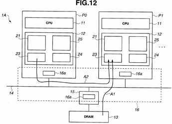
The bus?14?is a bus including a snoop mechanism?16?for coherency maintenance. Each processor and the bus controller15?are provided with a hardware circuit?16?a?for the snoop mechanism or a directory-based coherency management mechanism. Hereinafter, an example of snoop mechanism will be described; however, a structure that is almost the same as the snoop mechanism can also be provided by means of directory-based coherency management. Also, although not clearly indicated in?FIG. 12, the hardware circuit?16?a?includes an arbiter that determines "which processor ultimately receives write-back data" in relation to a "write-back data reception response" output by each processor. In the configuration illustrated in?FIG. 12, each processor can access to the?cache?memory?12?using a?virtual?address in a?virtual address space. Furthermore, the?cache?memory?12?performs a read of data from the DRAM?13?and a write of data to the DRAM?13?while performing TLB miss processing and?cache?miss processing for access from the CPU?11.
Although a case of two processors being provided will be described below, similar operation can be provided in a case of three or more processors being provided.
FIG. 13?is a flowchart illustrating processing for a?cache?miss in a processor.

When performing TLB rewrite processing, each processor performs rewrite processing for a TLB?virtual?page memory?21and a TLB?physical?page memory?22?in the?cache?memory?12, while not performing a write-back of data in a data memory23?and a rewrite of data in a TLB?physical?page CAM?25.
Now, it is assumed that a?cache?miss has occurred in a processor P1. When a?cache?miss has occurred, for refilling, the cache?memory?12?generates a?physical?address RA from a?physical?page number RP in the?physical?page memory?22?to perform memory access to the DRAM?13?(S201).
Memory access to the DRAM?13?is monitored by the snoop mechanism?16. When memory access occurs, the snoop mechanism returns a snoop response. As a result, the processor P1 determines whether or not a valid?physical?page RP for the?physical?address RA relevant to the memory access corresponds to a?physical?page RP in the TLB?physical?page CAM?25?in any of the other processors in the bus?14, not DRAM?13?(S202).
For example, it is assumed that a processor P0 includes the valid?physical?page RP. Such case may occur because although a write-back of data changed in the processor P0 should be performed when a TLB rewrite is performed, data remains in the data memory?23?until the write-back of the data is performed.
Accordingly, if the valid?physical?page RP for the?physical?address RA corresponds to a?physical?page RP in the TLB physical?page CAM?25?in any of the other processors (S202: YES), the corresponding processor (here, the processor P0) consults a state memory?24?for the relevant?cache?line, and if the?cache?state is not "Invalid", relevant data is transferred from the data memory?23, and thus, the?cache?memory?12?in the processor P1 obtains the data from the processor P0 (S203). The processor P1 can obtain data through a route indicated by an arrow A2 in?FIG. 12.
In this case, no access from the processor P1 to the DRAM?13?occurs, and thus, the processor P1 can obtain data at high speed by means of data transfer from the processor P0. Consequently, a processor with enhanced task switching responsiveness can be provided.
As described above, task switching processing according to the present embodiment enables provision of a?virtual address?cache?memory and processor with enhanced task switching responsiveness using a?cache?memory enabling reduction of the circuit amount by providing a TLB function in the?cache?memory.
II) Write-Back Processing of Data in a Multiprocessor System
Next, write-back processing of data in a multiprocessor system according to the present embodiment will be described.
An above-described?cache?memory can be applied to each processor included in a multiprocessor system or a multicore system.
In a multiprocessor system?1A including the configuration illustrated in?FIG. 12, a processor may perform a write-back (i.e., castout) of data to the DRAM?13. For example, when a?cache?miss occurs in the?virtual?address?cache?memory?12?in a processor, the processor writes data in the data memory?23?back to the DRAM?13, which is a main memory.
Conventionally, a write-back of data to a main memory should be performed without fail, and thus, when the amount of data transferred to the main memory increases, a decrease in the performance of the overall system and an increase in power consumption due to transfer processing inevitably occur.
Therefore, in the present embodiment, a write-back of data is performed by transferring the data to a?cache?memory in another processor, not a main memory, enabling preventing a decrease in performance of the overall system, and also enables reduction of power consumption for transfer processing.
Here, for example, it is assumed that a?cache?miss occurs in the processor P1 and the processor P1 performs a write-back of data in a?physical?address RA. The processor P1 outputs data relevant to processing for a write-back of data to the DRAM?13, to the bus?14.
The data in the bus?14?is monitored by the snoop mechanism?16, and other processors are notified of the data by the snoop mechanism?16.
For example, the processor P0 performs processing in?FIG. 14?based on the notice.?FIG. 14?is a flowchart illustrating an example of write-back processing upon occurrence of a?cache?miss. The processing in?FIG. 14?is performed by the hardware circuit in the?cache?memory?12. Furthermore, a below-described function of the snoop mechanism?16?is provided by extending a function of the snoop mechanism?16. In other words, the snoop mechanism?16, which is a coherency-maintenance protocol mechanism, monitors whether or not there is write-back data targeting the DRAM?13, and when the snoop mechanism?16?detects the write-back data, notifies processors other than the processor that has generated the write-back data.

The processor P0, based on the write-back data included in the notice received via the bus?14, determines whether or not there is a?physical?page RP in its own TLB?physical?page CAM?25?corresponding to a?physical?page RP for a write-back destination?physical?address RA (S301).
If there is a corresponding page (S301: YES), whether or not a corresponding entry in a TLB?virtual?page memory?21?is in a valid state is determined (S302).
If it is in a valid state (S302: YES), whether or not a relevant entry in the?cache?state memory?24?is "Invalid" is determined (S303).
If it is "Invalid" (S303: YES), whether or not the processor P0 itself has the highest priority among the processors that can receive the write-back data is determined (S303A). If the processor P0 itself has the highest priority (S303A: YES), the write-back data is transferred to the relevant data memory?23?in the?cache?memory?12, and changes the?cache?state from "Invalid" to "Modified" (S304).
In the case of "NO" in S301, S302, S303?or S303A, the processing is ended without doing anything. Where a protocol allowing a "Dirty-Shared" state such as MOESI, is employed, it should be understood that it is possible to perform optimization according to the coherence protocol such as a "processor having the highest priority" determined in S303A "transfers the write-back data to a relevant?cache?and changes the?cache?state to ‘Owned‘" in S304, and a "processor other than the processor having the highest priority" "transfers the write-back data to a relevant?cache, and changes the cache?state to ‘Shared‘" in S304.
In other words, where a same?physical?address is included in the TLB?physical?page CAM?25, the relevant data in TLB virtual?page memory?21?is valid and the relevant data in the data memory?23?is invalid, an area in which a corresponding entry exists but no data is stored exists in the?cache?memory?12?in the processor P0. In such case, the processor P0 transfers the write-back data to the?cache?memory?12?to store the write-back data in the?cache?memory?12.
Next, processing in a memory controller?15, which is a control section for a main memory, will be described.
FIG. 15?is a flowchart illustrating processing performed by the memory controller?15?for a write-back.

The memory controller?15?loads the write-back data from the processor P1 (S311).
Next, the memory controller?15?makes an inquiry to all the processors via the snoop mechanism?16?as to whether or not the processors loaded the write-back data (S312). In response to the inquiry, the snoop mechanism?16?generates a response and returns the response to the memory controller?15. In other words, the snoop mechanism?16, which is a coherency-maintenance protocol mechanism, notifies the memory controller?15?of the write-back data being loaded to a cache?memory in another processor, in response to the inquiry from the memory controller?15.
Then, the memory controller?15, based on the response to the inquiry, determines whether or not any of the processors has loaded the data in its?cache?memory?12?(S313).
If none of the processors has loaded the data in its?cache?memory?12?(S313: NO), processing for writing the data to the DRAM?13?is performed (S314).
If any of the processors has loaded the data in its?cache?memory?12?(S313: YES), the memory controller?15?terminates the processing.
FIG. 16?is a diagram illustrating a manner of data write-backs. As illustrated in?FIG. 16, in the case of "NO" in S313, the write-back data from the processor P1 is transferred to the DRAM?13?as indicated by a dotted arrow A3, while in the case of "YES" in S313, the write-back data is transferred to the processor P0 as indicated by a solid arrow A4.
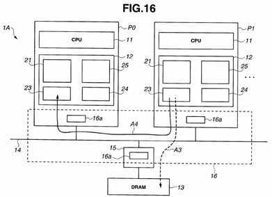
Occurrence of processing for writing data to the DRAM?13?leads to a decrease in the overall performance and an increase in power consumption for transfer processing. According to the present embodiment, where the write-back data has been loaded in the?cache?memory?12?in any of the processors, the memory controller?15?does not perform a write-back of the data to the main memory.
Consequently, a multiprocessor system according to the present embodiment, the above-described data write-back processing is performed, enabling reduction of the amount of access to the main memory by the respective processors for data write-back processing.
A multiprocessor system in which a TLB function is provided in a?cache?memory, enabling reduction of the circuit amount, and further enables reduction of the amount of access to a main memory by respective processors for data write-back processing can be provided.
Although in the above-described example, where the write-back data has been loaded in the?cache?memory?12?of any of the processors, the memory controller?15?does not perform a write-back of the data to the main memory, but the memory controller?15?may perform a write-back to the main memory.
III) DMA Processing
DMA processing according to a present embodiment will be described.
FIG. 17?is a block diagram illustrating a configuration of a multiprocessor system?1B including a plurality of processors. InFIG. 17, components that are similar to those in?FIG. 12?are provided with the same reference numerals, and a description thereof will be omitted. In the multiprocessor system?1B illustrated in?FIG. 17, each processor can perform data transfer to/from a DRAM?13?by means of DMA. For such purpose, each processor is provided with a DMA controller (hereinafter abbreviated as "DMAC")?26. The DMAC?26?is a DMAC including a memory management unit (hereinafter referred to as "MMU") including a TLB.

Conventionally, DMA transfer between a processor and the DRAM?13?is performed by designating a transfer source address and a transfer destination address using?physical?addresses; however, here, the DMAC?26?performs DMA transfer between the DRAM?13?and a?cache?memory?12A using?virtual?addresses for a?virtual?space.
FIG. 18?is a configuration diagram of a?cache?memory including a function that performs DMA transfer. In?FIG. 18, components that are the same as those in?FIG. 2?are provided with the same reference numerals, and a description thereof will be omitted.

A?cache?memory?12A, which is illustrated in?FIG. 18, includes a multiplexer (MUX)?41?and an arbiter?42?as an input section that inputs a?virtual?address. The arbiter?42?is connected to the multiplexer?41. The arbiter?42?monitors signals from a CPU11?and the DMAC?26, and determines whether a?virtual?address to be input to the?cache?memory?12A is a signal supplied from the CPU?11?or a signal supplied from the DMAC?26, and based on the determination result, outputs a selection signal SS to the multiplexer?41?so as to select a?virtual?address to be input. The multiplexer?41, based on the selection signal SS, switches input signals. In other words,?virtual?addresses EA from the CPU?11?and the DMAC?26?are input to the multiplexer?41, and either selected one of the?virtual?addresses EA is input to the?cache?memory?12A.
(GET Operation)
A GET operation in which a processor transfers data from the DRAM?13, which is a main memory, to its?cache?memory12A by means of DMA transfer will be described. The DMAC?26?in?FIG. 17?includes a memory management unit (hereinafter abbreviated as "MMU"). A transfer source address (source address) SA and a transfer destination address (destination address) DA are input to the DMAC?26?as?virtual?addresses.
For example, a CPU?11?in a processor P0 supplies the transfer source address SA and the transfer destination address DA, which are?virtual?addresses, to its DMAC?26. Then, the DMAC?26?searches out a?physical?address storage area holding latest data indicating the transfer source address SA using a snooping-based?cache?coherency mechanism and its MMU, and transfers the data to the transfer destination address DA in its own?cache?memory?12?by means of DMA transfer.
A storage area for the transfer destination address DA in a data memory?23?in the?cache?memory?12A in the processor P0 is allocated to the transferred data, and the transferred data is written to the storage area. Also, if there is an entry in the transfer destination address DA in the?cache?memory?12A, the transferred data is written in the storage area for the entry. Then, in the?cache?memory?12A, a dirty bit is written to the entry for the area with the transferred data written therein in the data memory?23.
As described above, a GET operation is performed to store transfer data in the?cache?memory?12A, enabling the CPU?11to read and process the data. Also, where a relevant storage area already exists in the?cache?memory?12A, no other data existing in the?cache?memory?12A is evicted.
Accordingly, when the DMA transfer is finished, data for the transfer destination address DA in the GET operation exists in the?cache?memory?12A, and thus, it can be expected that the?cache?hit rate is raised in subsequent accesses by the processor.
Next, processing in a GET operation will be described in detail.
FIG. 19?is a flowchart illustrating processing in a GET operation using DMA.
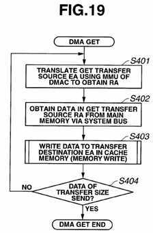
As illustrated in?FIG. 19, first, the DMAC?26?translates a transfer source address SA, which is a?virtual?address in a GET operation, using its own MMU to obtain a?physical?address RA (S401). Since DMA processing written in a program executed by the CPU?11?is written using?virtual?addresses, a?virtual?address is translated to a?physical?address in the DMAC?26.
The DMAC?26?obtains data in the transfer source address SA obtained in S401, which is a?physical?address in the GET operation, from the DRAM?13?via the bus?14, which is a system bus (S402).
Next, a transfer destination address DA, which is a?virtual?address from the DMAC?26, is input to the?cache?memory?12A, and transfer data is rewritten to a relevant storage area in the data memory?23?(S403). The processing in S403?is similar to memory write processing in?FIG. 7. In the?cache?memory?12A, in memory write processing, a dirty bit is written in an entry for an area of the data memory?23?in which the transfer data is written.
Then, the DMAC?26?determines whether or not data of a designated transfer size has been sent (S404).
If data of a designated transfer size has not been sent (S404: NO), the processing returns to S401. If data of a designated transfer size has been sent (S404: YES), the processing is ended. Since in DMA transfer, data is transferred in units of cache?line size, the determination in S404?is made per data of 128 bytes.
As a result of the above-described GET operation, data within a?cache?memory size can be transferred to the?cache memory?12A.
Accordingly, even if a program is a program of a size smaller than the memory size of the?cache?memory?12A and the program itself is one that is not intended to be executed using?virtual?addresses, that is, one that is executed in a?physical address space, the program can be executed using the?virtual?address?cache?memory?12A in the present embodiment. For example, where the memory size of the?cache?memory?12A is 256 KB and the size of the program is also 256 KB, addresses for the program are translated to?virtual?addresses of a size of within 256 KB in a?virtual?address space, enabling the program to be executed by a processor according to the present embodiment. The program is gotten by the cache?memory?12A by means of DMA transfer and executed.
(PUT Operation)
Next, a PUT operation will be described.
When a processor performs a PUT operation in which data in its?cache?memory?12A is transferred to the DRAM?13?by means of DMA, first, whether or not the data in the?cache?memory?12A, which is a transfer source address SA, is the latest by confirming the state data in the?cache?state memory?24, and if it is not the latest, confirmation is made using the snoop mechanism?16, which is a coherency-maintenance protocol mechanism. The DMAC?26?reads the latest data in the transfer source address SA, and transfers the latest data to the transfer destination address DA by means of DMA.
If a data entry for the transfer source address SA exists in the?cache?memory?12A, the data in the?cache?memory?12A is used for the data for the transfer source address SA. However, there may be a case in which no latest data for the transfer source address SA exists in the?cache?memory?12A. In such case, the DMAC?26?retrieves a value from the DRAM?13?via the bus?14, but does not put an entry for the value in the?cache?memory?12A and obtains the data only.
Also, since the transfer destination address DA is also a?virtual?address, if the latest data in the transfer destination address DA exists in the?cache?memory?12A, which corresponds to the DRAM?13, the corresponding data in the?cache memory?12A is invalidated, and the transfer data is written to the DRAM?13?or an entry in a?cache?memory?12A of another processor is updated and the transfer data is written to a data memory?23?of such other processor, using a?cache coherency protocol mechanism in the bus?14.
As a result of the above-described operation, if no latest data for the transfer source address SA exists in the?cache memory?12A, a PUT operation is performed without evicting the entries already existing in the?cache?memory?12A.
FIG. 20?is a flowchart illustrating processing in a PUT operation by means of DMA.

As illustrated in?FIG. 20, first, a transfer source address SA, which is a?virtual?address, is read from the data memory?23?in the?cache?memory?12A (S411). The processing in S411?is similar to the memory read processing in?FIG. 3.
Whether or not there is a?cache?hit in the?cache?memory?12A is determined (S412).
If there is a?cache?hit (S412: YES), processing for a?cache?read is performed (S413). The processing in S413?is similar to processing for a?cache?read in?FIG. 6. After S413, the processing moves to S416.
If there is no?cache?hit (S412: NO), the DMAC?26?translates a transfer source address SA, which is a?virtual?address, using its own MMU to obtain a?physical?address RA (S414).
The DMAC?26?obtains data in the transfer source address SA, which is the?physical?address obtained in S414, from the DRAM?13?via the bus?14?(S415).
Next, the DMAC?26?translates a transfer destination address DA, which is a?virtual?address, using its own MMU to obtain a physical?address RA (S416).
The DMAC?26?writes the data to the transfer destination address DA, which is a?physical?address, obtained in S416?from the DRAM?13?via the bus?14?(S417).
Then, the DMAC?26?determines whether or not data of a designated transfer size has been sent (S418).
If data of a designated transfer size has not been sent (S418: NO), the processing returns to S411. If data of a designated transfer size has been sent (S418: YES), the processing is ended. Since DMA transfer is performed in units of?cache?line size, the determination in S418?is performed per data of 128 bytes.
(Case of Prefetch)
Here, a case where data is prefetched into the?cache?memory?12A, that is, a case where a transfer source address SA and a transfer destination address DA in DMA transfer are the same will be described.
For example, when data in a?virtual?address in the?cache?memory?12A is invalid, there may be a case where the latest data is transferred to the?cache?memory?12A in advance so that the CPU?11?can immediately use the data after the transfer.
In such case, the invalid data in the?virtual?address is updated, and thus, the transfer source address SA and the transfer destination address DA in DMA transfer are the same. As a result, the latest data is transferred by means of DMA transfer to the?virtual?address in the?cache?memory?12A.
FIG. 21?is a flowchart illustrating processing in a GET operation for a prefetch.

As illustrated in?FIG. 21, first, the DMAC?26?determines whether or not a transfer source address SA and a transfer destination address DA are a same?virtual?address (EA) (S421). If they are not a same?virtual?address (S421: NO), the processing moves to the processing in a GET operation in?FIG. 19.
If they are a same?virtual?address (S421: YES), the processing for a memory read 2 is performed (S422).
Then, the DMAC?26?determines whether or not data of a designated transfer size has been sent (S423).
If data of a designated transfer size has not been sent (S423: NO), the processing moves to S421. If data of a designated transfer size has been sent (S423: YES), the processing is ended.
FIG. 22?is a flowchart illustrating processing in a memory read 2 in S422?in?FIG. 21.?FIG. 22?indicates a content that is substantially the same as the processing for a memory read in?FIG. 3, and the same processing steps are provided with the same step numbers, and a description thereof will be omitted.?FIG. 22?is different from?FIG. 3?in that processing for a cache?read (S5) is changed to processing for a?cache?read 2 (S431), which will be described below. Furthermore, whether or not the memory read is one targeting a source in a PUT operation using DMA transfer (transfer source address SA) is determined (S432). If the memory read is one targeting a source in a PUT operation using DMA transfer (S432: YES), the processing is ended, and if it is not, the processing moves to step S4.

FIG. 23?is a flowchart illustrating processing in a?cache?read 2 in S431?in?FIG. 22.?FIG. 23?indicates a content that is substantially the same as the processing for a?cache?read in?FIG. 6, and the same processing steps are provided with the same step numbers, and a description thereof will be omitted.?FIG. 23?is different from?FIG. 6?in that?FIG. 23?does not have S49?and S50?in?FIG. 6?because such steps are unnecessary where a transfer source address SA and a transfer destination address DA are the same in DMA transfer, that is, in prefetch processing.

Also, when GET and PUT operations using DMA are performed, the contents of TLB registration processing (FIG. 4), thecache?read processing (FIG. 6) and the?cache?write processing (FIG. 8) are changed as follows.
FIG. 24?is a flowchart illustrating the flow of TLB registration processing including DMA processing.?FIG. 24?indicates a content that is substantially the same as the TLB registration processing in?FIG. 4, and the same processing steps are provided with the same step numbers, and a description thereof will be omitted.?FIG. 24?is different from?FIG. 4?in that after S16, whether or not an address for the entry is a source in a DMA PUT operation, that is, a transfer source address is determined (S441). If the address is a transfer source address (S441: YES), a notice of a TLB miss and the relevant physical?page number RP is sent to the DMAC?26?(S442), and the TLB registration processing is ended. If the address is not a transfer source address (S441: NO), the processing moves to S17.

FIG. 25?is a flowchart illustrating?cache?read processing including DMA processing.?FIG. 25?indicates a content that is substantially the same as the processing for a?cache?read in?FIG. 6, and the same processing steps are provided with the same step numbers, and a description thereof will be omitted.?FIG. 25?is different from?FIG. 6?in that: while the processing in?FIG. 6?is performed by a?cache?controller, the processing?FIG. 25?is performed by the DMAC?26; and after S44, whether or not an address for the entry is a source in a DMA PUT operation, that is, a transfer source address is determined (S451).
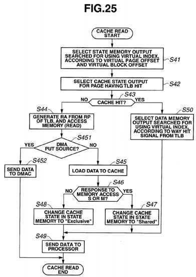
If the address is a transfer source address (S451: YES), data in the data memory?23?is sent to the DMAC?26?(S452), and the processing is ended. If the address is not a transfer source address (S451: NO), the processing moves to S45.
FIG. 26?is a flowchart illustrating?cache?write processing including DMA processing.?FIG. 26?indicates a content that is substantially the same as processing for a?cache?write in?FIG. 8, and the same processing steps are provided with the same step numbers, and a description thereof will be omitted.?FIG. 26?is different from?FIG. 8?in that: while the processing in?FIG. 8?is performed by a?cache?controller, the processing in?FIG. 26?is performed by the DMAC?26; and after S73, whether or not the?cache?write is a request from the DMAC as well as a write to all the?cache?lines is determined (S461).

If the?cache?write is a request from the DMAC?26?as well as a write to all the?cache?lines (S461: YES), the processing moves to S79. If the?cache?write is neither a request from the DMAC?26?nor a write to all the?cache?lines (S461: NO), the processing moves to S74.
Also, in the data write processing in S81?after S79, if the data is one from the DMAC?26, the data from the DMAC?26?is written to the?cache?memory?12A (S462).
As described above, data transfer between a?cache?memory and a main memory can be performed using?virtualaddresses by means of DMA processing, enabling provision of a processor capable of enhancing a?cache?hit rate in DMA transfer and a?cache?hit rate when the corresponding processor accesses the?cache?memory after DMA transfer.
IV) Application to a?Cache?Memory of Level 2 or Lower
Next, a processor according to a present embodiment will be described. Here, a description will be given taking a multiprocessor system using multilevel caches as an example.
FIG. 27?is a block diagram illustrating a configuration of a multiprocessor system?1C including a processor including multilevel?cache?memories. As illustrated in?FIG. 27, the multiprocessor system?1C includes a plurality of processors P11, P12, . . . , each having an L1?cache?51, one L2?cache?52?connected to the L1?cache?51?of each of the plurality of processors, and DRAMs?13?as one or more main memories connected to the L2?cache?52. Note that the main memory may be organized by physically and/or logically plural portions. The multiprocessor system?1C may be formed in one semiconductor chip in its entirety, or may also be partially formed in another semiconductor device.

In the case of a processor including multilevel caches (for example, a processor including an L1?cache?and an L2?cache), conventionally, in order to avoid occurrence of an alias in the L2?cache, access to the L2?cache?is performed using aphysical?address. Also, in order to avoid occurrence of an alias in the L1?cache,?physical?addresses are used for coherency management of the L1?cache.
In such processor, when the L1?cache?is accessed by the CPU, in most cases, a TLB in a MMU, which is provided separately from the L1?cache, is referred to. This is because: there is a high frequency of access to the L1?cache; and as can be seen in FIG. 5.28 in Computer Architecture—A Quantitative Approach—Forth Edition, the latency of the L2?cacheis often no more than around 25 cycles, and thus, when an L1?cache?miss occurs, it is necessary to immediately access the L2?cache. Accordingly, there is a problem that a large amount of power is consumed by the TLB hardware in the processor.
Therefore, the present embodiment is intended to provide a processor and a processor system enabling reduction of power consumption of TLB hardware.
FIG. 28?is a configuration diagram of a L2?cache?52. In?FIG. 28, components that are the same as those in?FIG. 18?are provided with the same reference numerals, and a description thereof will be omitted.

In?FIG. 28, an arbiter?42?is connected to a multiplexer?41. The arbiter?42?monitors a signal from each processor, and determines which processor supplied each?virtual?address EA input to the L2?cache?52, and based on the determination result, outputs a selection signal SS to the multiplexer?41?so as to select a?virtual?address EA to be input. The multiplexer41?switches input signals based on the selection signal SS.
The L1?cache?51?is a?cache?not including TLB hardware. The CPU of each processor accesses the L1?cache?51?using avirtual?address, and since the L1?cache?51?does not include TLB hardware, in the case of a?cache?miss, access to the L2cache?52?is performed using the?virtual?address. The L2?cache?52?includes a configuration that is substantially similar to, e.g., the above-described?cache?memory?12, and the L2?cache?52?is accessed using a?virtual?address, and accesses the DRAM?13?using a?physical?address.
Also, since the L2?cache?52?is a?cache?for the L1?cache?51?in each of the plurality of processors P11, P12, . . . ,?cache?data is managed and identified in the L2?cache?52?in association with the respective processors, and a process number PID includes information on a processor identifier.
Furthermore, a?cache?state memory?24?in the L2?cache?52?manages not only a?cache?state of the L2?cache?52, but also acache?state of the L1?cache?51.
For that purpose, a snoop mechanism?16A, which is a coherency-maintenance protocol mechanism for maintaining the coherency of?cache?data between the plurality of L1 caches?51?and the L2?cache?52, is provided between each processor and the L2?cache?52.
Accordingly, the?cache?state memory?24?is extended so as to include a storage area for storing?cache?states for each L1cache?51?and way information for each L1?cache?51.
An operation of the L2?cache?52?is similar to the operation illustrated in the flowcharts in?FIGS. 3 to 11.
As shown in Figure 5.29 in "Computer Architecture—A Quantitative Approach—Fourth Edition" (Hennessy, et al.), if the cache?hit rate of the L1?cache?51?is, for example, 95% or more, the rate of access to the L2?cache?52?is 5% or less. Accordingly, since the TLB is referred to only in the L2?cache?52, power consumption for referring to the TLB is reduced.
The above-described example is a multiprocessor system in which an L1?cache?in each of a plurality of processors is connected to one L2?cache. However, a similar effect can be provided for a processor including one L1?cache?and one L2cache, the L2?cache?having a configuration similar to the above-described configuration.
Also, although the above-described example has been described in terms of L1 and L2 caches, a similar effect can be provided between low-order caches of level 2 or lower like L2 and L3 caches in a processor or a multiprocessor with a configuration similar to that of the above-described L2?cache?52?provided to the lower-order?cache.
Next, variations of the above-described configuration of the L2?cache?52?will be described. Hereinafter, each variation will be described mainly in terms of differences from the above-described configuration of the L2?cache?52, and a description of components provided with the same reference numerals will be omitted.
(Variation 1)
A basic configuration of a?virtual?address?cache?memory according to variation 1 is the same as that of the above-described L2?cache?52, but is different in an operation when an alias is detected.
In the embodiment, when an alias is detected, the L2?cache?52?performs processing for invalidating the TLB entry causing the alias as indicated in steps S17?onward in?FIG. 4.
In contrast, in variation 1, processing in S21?is not performed. In other words, a new entry is registered without invalidating the TLB entry causing the alias. In variation 1, an alias occurs in the?cache?and the TLB in one and the same processor; however,?cache?coherence control using snooping is applied also to the one and the same processor to overcome the alias. In other words, although a plurality of addresses causing an alias exist in the L2?cache?52, a coherence protocol is applied to each cash line causing an alias, maintain the coherency of the states of a plurality of?cache?lines.
For example, when a?physical?address subjected to a write by a process A is subjected to a read by a process B, the following operation will be performed. A case where immediately after the?physical?address is subjected to a write by a process A, the?physical?address is subjected to a read by a process B in one and the same processor will be considered. From a viewpoint of a?virtual?address in the process A, the?cache?state is "Modified", and from a viewpoint of a?virtual address in the process B, the?cache?state is "Invalid".
Accordingly, a?cache?miss occurs, and thus, the processing advances to S44?in?FIG. 6?to perform access to the DRAM?13.
Snooping is performed for the access to the DRAM. In other words, the TLB?physical?page CAM?25?in?FIG. 2?is accessed, and a TLB entry managed by the process A, that is, whose PID belongs to Process A, is hit. A?cache?line written by the process A is accessed, a "Modified" response is returned, and then data is output. The?cache?line managed by the process A enters a "Shared" state. The processor receives the "Modified" response and the data output by the process A. The cache?line managed by the process B issuing the request is loaded, and the?cache?state is changed to "Shared".
In variation 1, although a process A and a process B, which are performed by one and the same processor by means of time sharing, the operation is performed as if such processes are performed by separate processors.
In the case of the configuration in variation 1, multiple hits are allowed in the TLB?physical?page CAM?25. More specifically, one bit for each TLB entry is allocated to a hit output of the TLB?physical?page CAM?25, and the hit output is not encoded. Also, responding to the TLB?physical?page CAM?25?allowing multiple hits, the?cache?state memory?24?allows simultaneous access to all the entries. More specifically, the?cache?state memory?24?is organized by ordinary logic circuits, not SRAMs. Then, an output from the?cache?state memory?24?is encoded by, e.g., a priority encoder as with a state of a coherent bus. For state encoding, a method such as one in which a?cache?state is encoded so that one bit is allocated to each state, and a logical OR of all the entries in the state memory?24?causing an alias is obtained, thereby obtaining a state for the state memory?24?may be employed.
A?virtual?address?cache?memory according to variation 1 enables provision of an effect similar to that of the configuration of the L2?cache?52, and omitting processing for invalidating TLB entries causing an alias.
(Variation 2)
Although a basic configuration of a?virtual?address?cache?memory according to variation 2 is the same as that of the above-described L2?cache?52, in variation 2, a TLB entry is not rewritten even if an?index?in the TLB?virtual?page memory21?causing an alias and an?index?to be registered correspond to each other. In other words, each entry causing an alias in the TLB?virtual?page memory?21?is completely independently controlled, and alias processing in the TLB is eliminated, and the consistency between the entries causing an alias is left to a?cache?coherence mechanism.
In other words, variation 2 is different in that when an alias is detected, indexes in the TLB?virtual?page memory?21?are not checked.
In TLB entry registration processing in variation 2, processing in S17, S20, S21?and S22?in?FIG. 4?is excluded, and after processing in S16?and S24, processing in S18?and S19?is performed.
In the configuration in variation 2, restrictions on the hardware configuration are the same as those in variation 1, multiple hits are allowed in the TLB?physical?page CAM?25, and the?cache?state memory?24?can access a plurality of entries simultaneously.
According to variation 2, TLB entries are completely independently controlled, and a plurality of processes performed by one and the same processor exhibit operations that are completely the same as those performed by different processors.
Accordingly, in variation 2, an effect similar to that of variation 1 is provided, and when a plurality of processes are performed, TLB entries in the respective processes are not invalidated, reducing overhead for a TLB miss.
(Variation 3)
FIG. 29?is a configuration diagram of a?cache?memory according to variation 3.

As illustrated in?FIG. 29, the?cache?memory includes a TLB CAM?21A, a TLB?physical?page memory?22A, a data memory23A and a?cache?state memory?24A. The?cache?memory according to variation 3 is a full associative?cache.
For example, the?cache?memory is configured so that a full associative?cache?having a?cache?capacity of 256 KB and a cache?line size of 128 bytes is managed in units of 4 KB page size. It is supposed that page information, which is managed by the TLB, has 10 bits and a?cache?line state has 10 bits.
In such case, where a?physical?address and a?virtual?address are 40 bits and 32 bits, respectively, the size of the TLB CAM?21A in variation 3 can be figured out as follows:
physical?page number: 40 bits?12 bits=28 bits,?
virtual?page number: 32 bits?12 bits=20 bits,?
entry count: 256 KB/4 KB=64 entries,?
and therefore,

The size of a state memory (corresponding to a conventional?tag?memory) in a L1?cache?is substantially reduced sincecache?entry replacement is performed on a page basis.
In other words,

The present configuration requires?physical?page information, not requiring?virtual?page information, and thus,

Accordingly, in the following conditions:
The L1?cache?can be managed with a memory that is smaller than a conventional one. The reduction of a?tag?per content and the TLB content is due to association of tags in the L1?cache?with page numbers, thereby enabling the tags to be omitted.
Next, advantages will be described in terms of the performance. A condition in which two processes (having mutually-independent?virtual?address spaces) are performed by one and the same processor, and these two processes share a same?physical?address page for data reception/delivery will be considered. It is assumed that: the two process are a process A and a process B, respectively; a shared?physical?page is RP—1;?virtual?pages in the process A and in the process B corresponding to the shared?physical?page are EP—1A and EP—1B, respectively; and a page updated by the process A is read by the process B.
It is assumed that a write permission for this page is given to the process A, while a write permission for this page not being given to the process B. Furthermore, it is assumed that a page table is prepared in advance, and the?physical?page has not been used until the process A started to create data to be delivered to the process B. Also, it is assumed that the process A is closed when the process A finished the creation of data to be used by the process B and then the process B is used. It is assumed that the?cache?employs a write-allocate, write-back method.
A shared memory read and a shared memory write will be described below using?FIGS. 30 and 31.?FIG. 30?is a flowchart of a shared memory read in variation 3.?FIG. 31?is a flowchart of a shared memory write in variation 3.
As illustrated in?FIG. 30, when a memory read is started, the TLB?virtual?page memory?21A, the data memory?23A and the state memory?24A are accessed using a?virtual?index?(S201). If the TLB?virtual?page memory?21A has no hit (S202: NO), TLB registration processing for a read is performed. If the TLB?virtual?page memory?21A has a hit (S202: YES), the processing advances to S212.

More specifically, processing for reading a PTE (page table entry) to be registered is performed on the DRAM?13?(S203). Whether or not the PTE (page table entry) to be read exists in the DRAM?13?is determined (S204). If the PTE does not exist (S204: NO), a notice of occurrence of an exception is sent to the OS (S205).
If the PTE exists (S204: YES), whether or not to permit this process to perform a read is determined (S206). If the process is not permitted to perform a read (S206: NO), the processing advances to S205. If the process is permitted to perform a read (S206: YES), a reference bit in the PTE is set (S207), and the processing advances to S208.
Then, whether or not the read PTE and a?physical?page number for any of all the valid TLB entries correspond to each other in terms of?physical?page number is determined (S208). If the?physical?page numbers do not correspond to each other (S17: NO), TLB miss processing is performed (S209), a new PTE is registered as a TLB entry (S210), and the processing advances to S212.
On the other hand, if the?physical?page numbers correspond to each other (S208: YES), a?virtual?page number, a process number and protection information of the TLB entry having the corresponding?physical?page number are rewritten (S211), and the processing advances to S212.
In S212, whether or not a?virtual?page for the TLB entry is readable is determined. If the?virtual?page is not readable (S212: NO), a notice of a protection violation is sent by interrupt processing to the CPU?11?(S213), and exception processing is performed by the OS.
If the?virtual?page is readable (S212: YES), a?cache?read is performed. In other word, whether or not a?cache?hit occurs is determined (S214). If no?cache?hit occurs (S214: NO), a?physical?address is generated from the?physical?page number in the TLB to issue a memory access request (S215). Then, the obtained data is loaded to the?cache?memory (S216).
The memory access request is snooped by the memory and the other processors. Each of the processors that have snooped the memory access request checks the?cache?state managed by the processor itself, and if the?cache?state is "Modified", returns a "Modified" response as a snoop response, and if the?cache?state is "Exclusive" or "Shared", returns a "Shared" response, and thus, the processor that has issued the request updates the?cache?state in the?cache?state memory?24A according to the snoop response. In other words, if the snoop response is a "Shared" response or a "Modified" response (S217: YES), the state of the request target?cache?line in the?cache?state memory?24A is changed to "Shared" (S218), and if the snoop response is neither a "Shared" response nor a "Modified" response (S217: NO), the state of the request target?cache?line is changed to "Exclusive" (S219). Then, data is transmitted to the CPU?11?(S220).
If a?cache?hit occurs (S214: YES), the processing advances to S217.
As illustrated in?FIG. 31, when a memory write is started, the TLB?virtual?page memory?21A, the data memory?23A and the state memory?24A are accessed using a?virtual?index?(S221). If the TLB?virtual?page memory?21A has no hit (S222: NO), TLB registration processing for a write is performed.
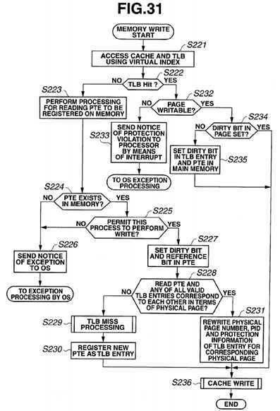
If there is a hit in the TLB (S222: YES), the case is determined as a case of a TLB hit, and whether or not the?virtual?page is writable is determined (S232). If it is writable (S232: YES), whether or not a dirty bit in the?virtual?page is set is determined (S234), if a dirty bit in the?virtual?page is not set (S234: NO), a dirty bit is set in the PTE in the TLB entry and the PTE in the DRAM?13, and a?cache?write is performed (S236). If a dirty bit in the?virtual?page is set (S234: YES), acache?write is performed (S236).
On the other hand, if the?virtual?page is not writable (S233: NO), a notice of a protection violation is sent to the CPU?11?by means of interrupt processing (S233), and exception processing is performed by the OS.
If there is no hit in the TLB (S222: NO), TLB registration processing is started, processing for reading a PTE to be registered is performed on the DRAM?13?(S223). Whether or not the PTE to be read exists in the DRAM?13?is determined (S224). If the PTE does not exist (S224: NO), a notice of occurrence of an exception is sent to the OS (S226).
If the PTE exists (S224: YES), whether or not to permit this process to perform a write is determined (S225). If the process is not permitted to perform a write (S225: NO), the processing advances to S226.
If the process is permitted to perform a write (S225: YES), a dirty bit and a reference bit in the PTE are set (S227).
Then, whether or not the read PTE and any of all the valid TLB entries correspond to each other in terms of?physical?page number is determined (S228). If the?physical?page numbers do not correspond to each other (S228: NO), TLB miss processing is performed (S229), a new PTE is registered as a TLB entry (S230), and the processing advances to S236.
On the other hand, if the?physical?page numbers correspond to each other (S228: YES), a?virtual?page number, a process number and protection information of the TLB entry having the corresponding?physical?page number are rewritten (S231), and the processing advances to S236.
As illustrated in?FIG. 32, when TLB miss processing is started, whether or not an unused TLB entry exists is determined (S241). If an unused TLB entry exists (S241: YES), the processing is ended.

If no unused TLB entry exists (S241: NO), a TLB entry to be evicted (S242) is determined, and whether or not "Modified"cache?lines exist in the TLB entry to be evicted is determined (S243). If no "Modified"?cache?lines exist (S243: NO), the processing is ended.
If "Modified"?cache?line exists (S243: YES), all the "Modified"?cache?lines in the page to be evicted are flashed (S244), and the processing is ended.
As illustrated in?FIG. 33, when TLB registration processing is started, processing for reading a PTE to be registered is performed on the DRAM?13?(S251). Whether or not the PTE to be read exists in the DRAM?13?is determined (S252). If the PTE does not exist (S252: NO), a notice of occurrence of an exception is sent to the OS (S253).

If the PTE exists (S252: YES), whether or not a cause of the TLB miss is a store instruction is determined (S254).
If the cause is not a store instruction (S254: NO), whether or not to permit this process to perform a read is determined (S257). If the process is not permitted to perform a read (S257: NO), the processing advances to S253. If the process is permitted to perform a read (S257: YES), a reference bit in the PTE is set (S258), and the processing advances to S259.
If a cause of the TLB miss is a store instruction (S254: YES), whether or not to permit this process to perform a write is determined (S255). If the process is not permitted to perform a write (S255: NO), the processing advances to S253.
If the process is permitted to perform a write (S255: YES), a dirty bit and a reference bit in the PTE are set (S256).
Then, whether or not the read PTE and any of all the valid TLB entries correspond to each other in terms of?physical?page number is determined (S259). If the?physical?page numbers do not correspond to each other (S259: NO), TLB miss processing is performed (S260), and a new PTE is registered as a TLB entry (S261).
On the other hand, if the?physical?page numbers correspond to each other (S259: YES), a?virtual?page number, a process number and protection information of the TLB entry having the corresponding?physical?page number are rewritten (S262).
As described above, when the process A starts creating data to be delivered to the process B, the process A accesses the TLB using a?virtual?index; however, a TLB miss occurs in S222?in?FIG. 31, and thus, a page table entry for associating a physical?page RP—1 with a?virtual?page EP—1A is called up in the TLB (S223). Here, a valid bit in the TLB entry is set and the state of each?cache?line for the page is "invalid". For the process A, a write bit of this page is set, and thus, the process A can perform a write to this page. Also, since no write to this page is performed at the start of the process, this page is clean; however, this page is accessed in a memory write, and thus, a dirty bit in the page is set (S235).
Since the write allocate method is employed, write target?cache?lines are read from the DRAM?13?(S215), and the TLB is rewritten to change the states of these?cache?lines to valid and dirty. Thereafter, if there is a?cache?hit in a write to the cache?by the process A, data in the?cache?is updated, and if there is a?cache?miss, data is allocated from the DRAM?13?to the?cache, and then the?cache?is updated. Since the write allocate method is employed, even though only a part of the cache?lines is updated, the?cache?lines are kept in their latest states.
A state in which a write to a page by the process A is finished and the process A is switched to the process B is considered. It is assumed that until the start-up of the process B, the?physical?address RP1 is neither accessed nor evicted from the L1?cache. When the process B accesses a?physical?address RP—1 (S201), a miss occurs for a?virtual?address since the process number is different (S202); however, a hit occurs for the?physical?address (S208). Therefore, the TLB performs operations necessary for process switching such as changing the?virtual?page number from EP—1A to EP—1B and the process number from the process A to the process B without rewriting a valid bit and a dirty bit in the page, and clearing a write bit for the process B (S211). Here, what is rewritten is only the page information, and the?cache?lines are not rewritten and?cache?flash is not performed, either.
A case in which the process B accesses a?physical?address space RP—1 by designating a?virtual?address space EP—1B will be considered. Although the process number and?virtual?page information in the TLB has been rewritten, the page table in the TLB has been maintained, and the content in the L1?cache?is also maintained, and thus, the process B can read information written by the process A from the?cache. For an area in one and the same page in which the process A has not performed a write, the?cache?line states are "Invalid", and thus, a?cache?miss occurs; however, correct data can be read by data from the memory being allocated to the?cache.
As described above, the process B can read data shared by the process A from the?cache?without causing an unnecessary?cache?miss and/or TLB miss.
Where it is necessary to invalidate a TLB entry, e.g., where RP—1 is a target for replacement because of another TLB miss, a correct operation of the system can be ensured by performing the following operation.?FIG. 32?is a flowchart for TLB miss processing in variation 3.?FIG. 33?is a flowchart of TLB registration processing in variation 3.
Referring to a TLB entry in variation 3, whether or not?cache?lines are valid and have dirty data can be clarified. The?cachelines are written back to the main memory and valid bits in the?cache?lines are cleared (S244?in?FIG. 32).
Also,?cache?flash is performed until no dirty?cache?lines appear in the page. Also, when the?cache?flash in the page is finished, the page is invalidated. The replacement target page table entry is registered in the TLB (S230?in?FIG. 31).
In variation 3, when a TLB miss occurs, a check of "whether or not there is an entry having a RP hit exists in the TLB" is added (S208?and S228), if there is, processing for rewriting a part of the TLB entry is added (S211?and S231). Conventionally, when a TLB miss occurs, very heavy processing such as TLB miss processing and TLB registration occurs unconditionally. Also, when the process B starts accessing the shared memory, heavy processing such as invalidation of a TLB entry for the process A, and?cache?flash of the content of the page indicated by the entry always occurs for the shared memory space. On the other hand, according to variation 3, it is highly possible that relatively light processing such as rewriting the TLB entry is used.
In variation 3, the?cache?state can be managed on a page basis. When the?cache?state is managed on a page basis, thecache?state memory?24A is configured to have one?cache?state for an entire page, not for each page offset. In other words, the?cache?state memory?24A has one state according to a coherency protocol, for example, the MESI protocol, for an entire page without decoding a page offset (0-31). Where the?cache?states are managed on a page basis, also, the data memory, as in?FIG. 29, is accessed by providing an offset in the page like an address (11:0) to the data memory. In other words, such page-based?cache?state management can be provided with a configuration that is completely the same as that in?FIG. 29?other than the?cache?state memory.
As described above, a?virtual?address?cache?memory according to variation 3 enables provision of an effect similar to that provided by the L2?cache?52, also using a full associative?cache.
(Variation 4)
FIG. 34?is a configuration diagram of a?cache?memory according to variation 4.

As illustrated in?FIG. 34, the?cache?memory includes a TLB CAM?21B, a TLB?physical?page memory?22B, a data memory23B, a?cache?state memory?24B and a TLB?physical?page CAM?25B. The?virtual?address?cache?memory according to variation 4 is also a full associative?cache.
In variation 4, snooping can be performed by the TLB?physical?page CAM?25B.
In variation 4, access from the processor core side using a?virtual?address is substantially similar to that of variation 3 with no snoop mechanism provided, and thus, a description thereof will be omitted. When there is access from a processor bus using a?physical?address, a?cache?state check is performed in the following procedure.
Bits (39:12) corresponding to a page number for the?physical?address from the processor bus are input to the TLB?physicalpage CAM?25B. If there is a matching?physical?page in the TLB?physical?page CAM?25, the TLB?physical?page CAM?25outputs an entry number. If there is no matching?physical?page, snooping is ended.
The?cache?state memory?24B is accessed using the entry number. Here, if such access conflicts with access from the CPU?11, snooping has a priority.
A?cache?state is checked using the?cache?state memory?24B. A snoop response is determined based on the?cache?state and the request, and the?cache?states are updated. If data transfer is needed because, e.g., the?cache?state is "Modified" according to the MESI protocol, data transfer is performed.
In response to a request from the CPU?11, a?cache?having the present configuration outputs a snoop request as described below.
The?cache?state memory?24B is accessed using bits (11:7) in a 31-bit?virtual?address from the CPU?11?to check the?cachestate. Since the?cache?is of a full associative type, there are 64?cache?state candidates.
Simultaneously, the TLB?virtual?page CAM?21B is accessed using a page number in bits (31:12) in the 31-bit?virtualaddress and a process number PID to check whether or not there is a corresponding entry, and if such entry exists, the TLB?virtual?page CAM?21B outputs an entry number. If no such entry exists, TLB miss processing is performed. A description of the case of a TLB miss will be omitted because it has already been provided.
In the case of a TLB hit, a?cache?state is selected from the?cache?state memory?24B using the entry number output by the TLB?virtual?page CAM?21B. If the?cache?state is "Modified (M)" or "Exclusive (E)", snooping is not required. In the case of a state other than those states, a snoop request is issued as necessary according to a request from the CPU?11, which is a processor core, and the?cache?state.
An example of the case requiring a snoop is a write to S state?cache?line or a?cache?miss occurring when a TLB hit occurs.
In a configuration employing snooping, for snooping, the TLB?physical?page CAM?25B is used to check whether or not a snooping target address exists in the?cache. The TLB?physical?page CAM?25B is also used to check whether a relevant entry exists in the TLB when a TLB miss occurs; however, a TLB miss does not frequently occur, and thus, there is only small overhead even if the TLB?physical?page CAM?25B is shared with snooping. Meanwhile, although the?cache?state memory?24B is frequently accessed because the?cache?state memory?24B is referred to for every data?cache?access, for snooping, unnecessary transactions are excluded in advance using the TLB?physical?page CAM?25B, and there is no need to check a?cache?state for a transaction that should not exist in the?cache, and therefore, only a small overhead is required.
As described above, a?virtual?address?cache?memory according to the variation 4 enables provision of an effect similar to that of the L2?cache?52?using a full associative?cache, too.
(Variation 5)
FIG. 35?is a configuration of a?cache?memory according to variation 5.

As illustrated in?FIG. 35, the?cache?memory includes a TLB CAM?21C, a TLB?physical?page memory?22C and a data memory?23C. The?virtual?address?cache?memory according to variation 5 is also a full associative?cache.
In variation 5, the TLB?physical?page memory?22C includes?cache?state information for each entry.
Variation 5 also enables provision of an effect similar to that of the L2?cache?52.
(Variation 6)
A?cache?memory according to variation 6 includes a secondary TLB in addition to a primary TLB. The secondary TLB is a memory that is not linked to?cache?data, or having a page table only and not having a translation mechanism.
The secondary TLB is of a 4 or more-way set associative type, which is the same as the primary TLB, and includes a number of entries that is larger than that of the primary TLB, and the primary TLB. Also, dirty bits and reference bits are managed by the secondary TLB.
In the?virtual?cache?memory configuration, the?cache?is a 4-way set associative?cache. The?cache?is subject to page-based replacement management, and the?cache?state is managed on a?cache?line basis. A countermeasure for an alias in variation 6 is taken as follows.
For example, if?virtual?indexes correspond to each other, e.g., a PID, a?virtual?page number and protection information of the relevant TLB entry are rewritten. If?virtual?indexes do not correspond to each other, the TLB entry causing an alias is not invalidated and is left as it is.
Also, where an alias occurs between different indexes,?cache?line-based coherency control is performed. For providing coherency between entries, a coherency mechanism in a processor bus is used. As a result, coherency is provided between the entries.
Variation 6 also enables provision of an effect similar to that of the L2?cache?52.
(Variation 7)
A?cache?memory according to variation 7 is a memory including a mechanism that, when TLB registration processing is performed, reads a page indicated by a registered TLB entry from a memory in a low priority order.
If a processor accesses a?cache?line in the page during the low-priority access, the?cache?line is accessed in a high priority order.
Variation 7 can also provide an effect similar to that of the L2?cache?52.
As described above, the L2?cache?52?and the L2 caches according to the variations thereof enable reduction of power consumption of TLB hardware.
Also, as described above, the respective variations can be applied not only to an L2?cache, but also to a low-order?cacheof level 2 or lower. In such case, also, the TLB is referred to only for the level that is applied to the lower-order?cache, and thus, power consumption for TLB reference can be reduced.
Furthermore, in a multiprocessor system such as one illustrated in?FIG. 27, an L2?cache?is provided for the L1 caches in the respective processors, eliminating the need to provide a TLB to each L1?cache, and furthermore, one L2?cache?is shared by a plurality of L1 caches, enabling reduction of the overall hardware amount.
Each of the above-described?cache?memories can be provided by hardware alone, and can be viewed as an ordinary processor including a?cache?and a TLB from software including an OS.
While a certain embodiment has been described, this embodiment has been presented by way of example only, and is not intended to limit the scope of the inventions. Indeed, the novel memories, processors, and multiprocessor systems described herein may be embodied in a variety of other forms; furthermore, various omissions, substitutions and changes in the form of the memories, processors, and multiprocessor systems described herein may be made without departing from the spirit of the inventions. The accompanying claims and their equivalents are intended to cover such forms or modifications as would fail within the scope and spirit of the inventions.
SRC=https://www.google.com.hk/patents/US20140164702
Virtual address cache memory, processor and multiprocessor
标签:des style blog http color io os ar strong
原文地址:http://www.cnblogs.com/coryxie/p/3976850.html