标签:des style blog http color io os java ar
In a particular embodiment, a circuit device includes a translation look-aside buffer (TLB) configured to receive a virtual address and to translate the virtual address to a physical address of a cache having at least two partitions. The circuit device also includes a control logic circuit adapted to identify a partition replacement policy associated with the identified one of the at least two partitions based on a partition indicator. The control logic circuit controls replacement of data within the cache according to the identified partition replacement policy in response to a cache miss event.
The present disclosure is generally related to a system and method of partitioned replacement for cache memory.
In general, a cache memory can be utilized in computing systems to reduce memory access latencies. Such computing systems can include personal computers, wireless processing devices (such as wireless telephones, portable digital assistants (PDAs), and other wireless devices), gaming systems, other electronic devices, or any combination thereof. Generally, the cache memory is located between a processor and a main memory. Data and/or instructions that are accessed by the processor may be fetched from the main memory and stored in the cache memory to reduce latency.
From a processor perspective, an access to the cache memory is typically much faster than an access to the main memory. If the processor cannot locate a data item or instruction in the cache memory, a cache miss occurs and the main memory is accessed to retrieve the data item or instruction, which is loaded into the cache memory. If the cache is full, the data item or instruction may replace an existing item in the cache memory.
However, in a multi-threaded processor that includes a shared cache, each thread may have access to the cache memory and each thread may experience cache misses that result in a new data item being loaded into the cache memory. Such replacements can result in deletion of data or instructions from the cache that may be needed by another thread. Such replacements can adversely impact the performance of other threads.
In a particular embodiment, a circuit device includes a translation look-aside buffer (TLB) configured to receive a virtual address and to translate the virtual address to a physical address of a cache having at least two partitions. The circuit device also includes a control logic circuit adapted to identify a partition replacement policy associated with the identified one of the at least two partitions based on a partition indicator. The control logic circuit controls replacement of data within the cache according to the identified partition replacement policy in response to a cache miss event.
In another particular embodiment, a method is disclosed that includes reading a translation look-aside buffer (TLB) entry to map a virtual address to a physical entry. The physical entry includes a partition indicator associated with a partition of a cache memory including at least two partitions. The method also includes selecting a cache replacement policy based on the partition indicator.
In still another particular embodiment, a method is disclosed that includes partitioning a cache memory into two or more partitions. A system configuration setting defines a size of each of the two or more partitions. The method also includes configuring a replacement policy associated with each of the two or more partitions.
One particular advantage provided by embodiments of the circuit device to determine a cache partition replacement policy is provided in that the circuit device can provide a guarantee of a quality of service (QoS) with respect to a high priority thread of a shared cache in a multi-threaded processor. For example, by controlling replacement of cache lines when a cache miss occurs, embodiments of a replacement control logic circuit disclosed herein may limit replacement to a particular partition within the cache. In this example, the replacement control logic circuit can reduce undesired replacement of data or instructions related to high priority threads by preventing replacement of data or instructions in a cache partition associated with the high priority thread.
Another particular advantage is provided in that the replacement policy for each partition of a partitioned cache may be different, allowing for higher Quality of Service
Other aspects, advantages, and features of the present disclosure will become apparent after review of the entire application, including the following sections: Brief Description of the Drawings, Detailed Description, and the Claims.
FIG. 1?is a block diagram of a particular illustrative embodiment of a processor including a cache memory replacement control circuit;
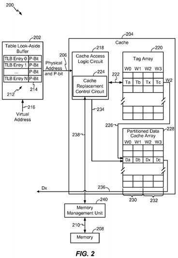
FIG. 2?is a block diagram of a second particular illustrative embodiment of a processor including a cache replacement control circuit;
FIG. 3?is a block diagram of a particular illustrative embodiment of a circuit device including a cache replacement control circuit;
FIG. 4?is a block diagram of a particular illustrative embodiment of a translation look-aside buffer including a partition bit;
FIG. 5?is a block diagram of a particular illustrative embodiment of a partitioned cache memory illustrating different replacement strategies applied to each partition;
FIG. 6?is a flow diagram of a particular illustrative embodiment of a method of controlling replacement of items in a partitioned cache memory;
FIG. 7?is a flow diagram of a particular illustrative embodiment of a method of partitioning a cache memory; and
FIG. 8?is a block diagram of a communications device that includes a partitioned cache memory and a cache replacement control logic circuit.
FIG. 1?is a block diagram of a particular illustrative embodiment of a processor100?including a cache memory replacement control circuit?104?to manage cache replacement within a partitioned cache. In a particular example, the processor100?may be a digital signal processor (DSP), a general-purpose processor, another type of processor, or any combination thereof. The processor?100includes a memory?102?that is coupled to a partitioned shared instruction cache110?and to a partitioned shared data cache?112?via a bus interface?108.
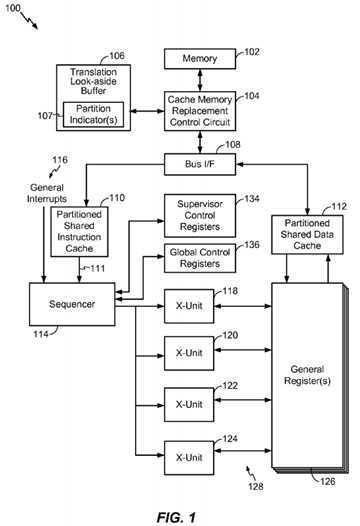
The cache memory replacement control circuit?104?is also coupled to the bus interface?108?and to a translation look-aside buffer (TLB)?106. The TLB?106includes one or more table entries for translation of a virtual memory address to a physical memory address. Each table entry includes a partition identifier (i.e. partition bit or P-Bit)?107?identifying a partition of the partitioned shared instruction cache?110?or the partitioned shared data cache?112. The cache memory replacement control circuit?104?is adapted to provide a virtual address to the TLB?106?and to receive a physical address and a partition identifier from the TLB?106. The cache memory replacement control circuit?104?permits replacement of an entry in an identified partition, within one of the partitioned shared instruction cache?110?or the partitioned shared data cache?112, based on the partition indicator?107. In particular, when a cache miss occurs that results in an access to the main memory?102, the cache memory replacement control circuit104?retrieves the partition indicator?107?from the TLB?106?and uses the partition indicator?107?to determine where a cache line replacement is permitted (i.e., in which partition the retrieved information may be written). In a particular embodiment, the cache memory replacement control circuit?104?may be integrated with the partitioned shared instruction cache?110, with the partitioned shared data cache?112, or any combination thereof.
The partitioned shared instruction cache?110?is coupled to a sequencer?114?via a bus?111. The sequencer?114?also receives general interrupts?116, which may be retrieved from an interrupt register (not shown). In a particular embodiment, the partitioned shared instruction cache?110?may be coupled to the sequencer?114?via a plurality of current instruction registers (not shown), which may be coupled to the bus?111?and associated with particular threads of the processor?100. In a particular embodiment, the processor?100?is an interleaved multi-threaded processor including six threads.
In a particular embodiment, the bus?111?is a one-hundred twenty-eight bit (128-bit) bus and the sequencer?114?is configured to retrieve instructions having a length of thirty-two (32) bits from the memory?102. The bus?111?is also coupled to a first instruction execution unit?118, a second instruction execution unit?120, a third instruction execution unit?122, and a fourth instruction execution unit?124. Each instruction execution unit?118,?120,?122,?124?is coupled to a general register file?126?via a bus, which is generally indicated at?128. The general register file?126?may also be coupled to the sequencer?114, the data cache?112, and the memory?102?via a second bus (not shown). The general register file?126?is coupled to the partitioned shared data cache?112?and is adapted to read data from and write data to the partitioned shared data cache?112.
The processor?100?may also include supervisor control registers?134?and global control registers?136?to store bits that may be accessed by control logic within the sequencer?114?to control execution of instructions. In a particular example, the supervisor control registers?134?and the global control registers?136?may include bits to configure partitions and partition sizes within the partitioned shared instruction cache?110?and the partitioned shared data cache?112. Additionally, the supervisor control registers?134?and the global control registers?136?may be accessible to the cache memory replacement control circuit?104. Particular bits within the supervisor control registers?134?and/or the global control registers?136?may specify a replacement control strategy to be used by the cache memory replacement control circuit?104?to replace particular lines within the partitioned shared instruction cache?110?and the partitioned shared data cache?112. In a particular example, the cache memory may be an n-way cache memory that is partitioned such that a first way of the n-way cache is associated with a first partition and a second way of the n-way cache is associated with a second partition. In a particular instance, the replacement control strategy may be partition specific, such that different replacement strategies can be used for replacement within different partitions. The replacement control strategies can be configured during an administrative operating mode. In a particular illustrative embodiment, particular applications may be able to configure the replacement control strategies during operation (i.e., on the fly) to enhance performance.
In a particular embodiment, the partitioned shared instruction cache?110?may be shared by the execution units?118,?120,122, and?124?and may be partitioned into two or more partitions. For example, the partitioned shared instruction cache?110may be partitioned into a first partition and a second partition, such as partitions?230?and?232?illustrated in?FIG. 2?and partitions?306?and?308?illustrated in?FIG. 3. In a particular example, higher priority threads may be assigned to the first partition, while lower priority threads or untrusted threads may be assigned to other partitions. On a cache miss related to a higher priority thread, such as a high priority processing thread, a new value is retrieved from the main memory?102, and the cache memory replacement control circuit?104?determines a cache partition bit and allocates the retrieved new value to a selected cache partition (e.g., the first partition?230) according to the cache partition bit. Additionally, the cache memory replacement control circuit?104?prevents other processes from replacing data or instructions in the selected partition. By selectively controlling replacement of cached instructions, quality of service may be enhanced for the high priority thread, since instructions for the high priority thread are not replaced by retrieved data related to a cache miss from another thread.
Similarly, data associated with a higher priority thread may be maintained in the shared partitioned data cache?112?that includes a first and second partition. By preventing lower priority threads from replacing the data in the first partition, the higher priority thread can trust that data in the first partition is not replaced based on a cache miss by a lower priority thread. Thus, quality of service for particular threads may be enhanced.
In a particular example, the cache memory replacement control circuit?104?may select a particular replacement algorithm based on the partition as determined from a partition indicator?107. For example, assuming the first partition is associated with a higher priority thread, the cache memory replacement control circuit?104?may select and utilize a "least frequently used"-type of replacement algorithm or a "round robin"-type of replacement algorithm for managing cache line replacements within the first partition. The cache memory replacement control circuit?104?may select a different replacement algorithm for the second partition. In a particular example, the cache memory replacement control circuit?104?can selectively apply one of a a round robin algorithm, a least frequently used replacement algorithm, a random replacement algorithm, or any combination thereof, for replacement of data or instructions in the second partition. In a particular instance, the cache memory replacement control circuit?104?may select a particular replacement algorithm based on a desired quality of service for a particular thread. The selected replacement algorithm may be used to determine which element of a memory to replace within a particular partition of the cache?110?or?112.
In a particular example, the cache memory replacement control circuit?104?may be included in a memory management unit (MMU) and the partition replacement control functions may be extended to other types of memory. In another example, a memory replacement control circuit, such as the cache memory replacement control circuit?104, may be adapted to control replacement access to a partition of a memory that has poor cacheability so that memory structures in a partition with poor cacheability do not evict information from structures with better cacheability in a different partition.
In another particular embodiment, the cache memory replacement control circuit?104?is adapted to monitor process usage and to dynamically adjust partition sizes and the partition replacement policies to provide a desired quality of service to particular threads. For example, certain tasks, such as higher priority tasks (e.g., real-time or near-real time executable instructions) may need a quality of service guarantee. Other types of code, such as Linux? operating system or application code JAVA?, and other code, may not be as well behaved and may try to consume a significant percentage of processor resources. The cache memory replacement control circuit?104?may dynamically adjust the size of a cache partition within one or both of the partitioned shared instruction cache?110?and the partitioned shared data cache?112. Such dynamic partitioning may be managed by adjusting page permissions within a global register or within the TLB?106, for example. By controlling replacement access to instructions within a particular partition of the cache, the higher priority task is guaranteed that expected data and instructions will not be overwritten by lower priority tasks, at least within the particular partition.
FIG. 2?is a block diagram of a second particular illustrative embodiment of a processor?200?including a cache replacement control circuit?224. The processor?200?includes a translation look-aside buffer (TLB)?202?that communicates with a cache memory?204?via a bus?206. The cache memory?206?also communicates with a memory management unit?240, which communicates with a main memory?208?via a bus?210.
The TLB?202?includes a TLB entry table?212?that includes a list of TLB entries. The TLB entry table?212?also includes a partition indicator?214, such as a partition bit (P-Bit). The TLB entry table?212?may also include a physical address, a page size, a cacheability indicator, and permissions, such as read, write, execute, other permissions, or any combination thereof. In a particular embodiment, each entry in the TLB entry table?212?has an associated partition indicator?214. In another particular embodiment, some of the entries in the TLB entry table?212?may have an associated partition indicator?214?and other entries may be assigned a default partition indicator. The TLB?202?also includes an input?216?to receive a virtual address. The TLB?202?is adapted to receive the virtual address at the input?216?and to translate the virtual address to a physical address with a partition indicator that can be provided to the cache?204?via the bus?206.
In a particular embodiment, the cache memory?204?is a multi-way (N-Way) cache that includes a cache access logic circuit218?that communicates with a tag array?220?via line?222. The cache access logic circuit?218?includes a cache replacement control circuit?224?that controls replacement of data within the cache?204?based on the partition indicator?214?received via the bus?206. The cache memory?204?also includes a partitioned cache data array?228, which communicates with the tag array?220?via line?226. In a particular embodiment, the cache memory?204?is a partitioned instruction cache array (such as the partitioned shared instruction cache?110?illustrated in?FIG. 1), a partitioned data cache array (such as the partitioned shared data cache?112?illustrated in?FIG. 1), or any combination thereof.
The cache access logic circuit?218?is responsive to physical address and partition indicator information received from the TLB?202. Each address from the TLB?202?includes a tag portion and an index portion, which may constitute a physical address, and a partition indicator?214?associated with that physical address. In a particular illustrative embodiment, the physical address may be a 32-bit address. In another particular embodiment, the partition indicator may include one or more bits to identify a partition within the cache memory?204.
In a particular embodiment, the cache access logic circuit?218?provides a control signal including an index value (Ix) and a tag value (Tx) to the tag array?220?via the line?222?to retrieve a plurality of tag values based on the input index value. Each of the tag values retrieved from the tag array?220?corresponds to a different one of a plurality of ways (such as way?0(W0), way?1?(W1), way?2?(W2), and way?3?(W3)) within the multi-way cache data array?228. The cache access logic circuit218?also provides an index value (Ix) to the partitioned cache data array?228?via line?234.
The input tag value (Tx) is compared to each of the plurality of tags from the tag array?220, based on the index value, to determine a matching tag and the associated identified way. In the particular illustrative example in?FIG. 2, the tag value Tx corresponds to way W2, which is associated with a second partition?232?of the cache data array?228. In this example, the identified way W2?is provided via line?226?to the cache data array?228. In the event that the tag array?220, does not contain a tag matching the tag value (Tx) at any associated way within the tag array?220?corresponding to the index value (Ix), then a cache miss has occurred. The cache access logic circuit?218?can receive the cache miss data from the tag array?220?via line?222?and a request to retrieve the data or instruction is made via line?238?to the memory management unit?240, which can retrieve the data and/or instruction from the external memory?208.
If there is a cache hit, meaning that the way is identified within the tag array?220, the information is received at the cache access logic circuit?218, which provides the index information (Ix) to the partitioned data cache array and the identified way value is provided to an input of the partitioned cache data array?228.
The cache data array?228?is partitioned into a first partition?230?and a second partition?232. For example, as shown in?FIG. 2, four different ways are shown (W0, W1, W2, and W3). In this example, the four ways (W0, W1, W2?and W3) are partitioned such that the ways W0?and W1?are associated with the first partition?230?and the ways W2?and W3?are associated with the second partition?232. When the cache data array?228?receives the index value and the way value via lines?234?and?226, identified data (Dx) can be retrieved from the second partition?232?and provided as an output via line236.
If the desired data is not found in the partitioned cache data array?228?or the way identifier is not found in the tag array?220, then a cache miss has occurred. The cache access logic circuit?218?sends a memory access request to the memory management unit?240?to retrieve the data or the instruction from the external memory?208. The memory management unit240?retrieves the data or the instruction from the memory?208?via a memory bus?210?and provides the information to the cache access logic circuit?218. The cache replacement control circuit?224?determines the partition indicator associated with the particular data or instruction to identify a partition within the cache data array?228?to which the data may be written. For example, if the cache miss occurred with respect to the second partition?232, the cache replacement control circuit?224?may identify the second partition?232?and write the data to the second partition. In particular, the cache replacement control circuit?224?determines whether to replace a line in the first partition?230?or the second partition?232?of the partitioned cache data array?228. Once the partition is identified (e.g., the second partition?232), the cache replacement control circuit?224identifies a replacement control policy associated with the identified partition.
The replacement control policy defines a replacement strategy for electing which particular line is to be replaced with the retrieved data or instruction. The replacement control policy may be a round robin replacement strategy that replaces an address line that is next in a round robin order (i.e., a round robin strategy may cycle through cache address lines starting at address line?0, continuing line by line until address line N is reached, and then cycling back to line?0?to start over). Another replacement control policy may be a least frequently used replacement strategy that includes identifying a least frequently used line in the cache of all of the available lines, and replacing the identified line. Other replacement strategies may also be used, such as random replacement. Another strategy may include making a probabilistic estimate of which cache lines may not be needed, for example, based on a partial decode of the contents of the cache line and assumptions about the types of processes currently running.
The cache replacement control circuit?224?may be adapted to apply a first replacement control strategy to the first cache partition?230?and a second replacement control strategy to the second cache partition?232. In a particular embodiment, the first cache partition?230?may be used to store instructions related to high priority processes or to a process that has a high quality of service requirement relative to other processes. The second cache partition?232?may be used to store instructions from other processes, which may have a lower priority or a lower quality of service. In this instance, the cache replacement control circuit may utilize a least frequently used replacement strategy to replace lines in the first cache partition?230, and use a random replacement strategy or round robin strategy with respect to replacement of lines in the second cache partition?232. In another embodiment, the cache replacement control circuit?224?may utilize a round robin replacement strategy for both the first and second cache partitions?230?and?232, but the replacement control circuit?224?may cycle through the first cache partition and the second cache partition differently. For example, if the partitioned cache includes a first partition that extends from cache line zero to cache line N and a second partition that extends from cache line O to cache line Z, the cache replacement control circuit?224?can replace data at the first cache partition?230?starting from line zero and proceeding to line N before cycling back and restarting at line zero. In contrast, the replacement control circuit?224may cycle through the second cache partition from line Z to line O and then restart at line Z. An example of these two different round robin replacement strategies is illustrated in?FIG. 5.
In a particular illustrative embodiment, the cache replacement control circuit?224?is configured to search the cache?204, including the tag array?220?and the partitioned cache data array?228, to identify an address match. The cache replacement control circuit?224?is adapted to identify a partition replacement policy associated with one of the partitions?230?and?232based on the partition indicator (P-Bit)?214. The cache replacement control circuit?224?applies the identified partition replacement policy to control replacement of data within the identified partition (e.g., the first cache partition?230) according to the identified partition replacement policy.
In a particular example, the cache access logic circuit?218?is adapted to permit read or write access to the partitioned cache data array?228?(to both the first and second partitions?230?and?232). However, the cache replacement control circuit224?prevents or limits replacement access to a particular partition (such as the first partition?230) based on the partition indicator?214. The partition indicator?214?identifies a particular partition (e.g., the first partition?230) within the partitioned data cache array?228. In a particular example, the cache access logic?218?is configured to reduce power consumption by disabling lookups to at least a portion of the partitioned data cache array (e.g., the second partition?232) that is not associated with the partition indicator (P-Bit?214), i.e., when the P-Bit?214?specifies the first partition?230. In a particular example, the cache access logic?218?may utilize the partition indicator to determine which of the partitions?230?and?232?is not used. In this instance, the cache access logic?218?can reduce power to the unused partition based on the partition indicator. In another particular example, the cache access logic?218?may include power control circuitry to selectively turn off power to a portion of a tag array?220, to a portion of a cache data array?228, or any combination thereof, within a cache memory?204.
FIG. 3?is a block diagram of a particular illustrative embodiment of a circuit device?300?including a cache memory control circuit. The circuit device?300?includes a cache memory replacement control circuit?302?that communicates with an N-way cache?304, which is partitioned. The N-way cache?304?includes a first partition (Partition A)?306, a second partition (Partition B)?308, and a third partition (Partition C)?310. The cache memory replacement control circuit?302?includes a cache replacement control circuit?312, a cache partition pointer selection logic circuit?314, replacement algorithms?316, a permissions logic circuit?318, a tag matching logic circuit?320, and a pointer reset logic circuit?322.
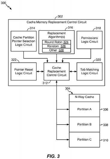
The cache replacement control circuit?312?is adapted to communicate with the tag matching logic circuit?320?to receive data related to a tag that does not match data stored at a tag array, such as the tag array?220?illustrated in?FIG. 2, indicating a cache miss. When data is retrieved based on a cache miss, the cache replacement control circuit?312?determines a partition indicator associated with the particular process that experienced the miss. Based on a partition indicator from a translation look-aside buffer (TLB), the cache replacement control circuit?312?determines a replacement algorithm?316. The replacement algorithms?316?may include a round robin algorithm?324, a random algorithm?326, and another algorithm?328(such as a least frequently used algorithm, a first in first out algorithm, or other algorithms). In another particular embodiment, the replacement algorithms may include a round robin algorithm?324, a random algorithm?326, another algorithm?328, or any combination thereof The cache replacement control circuit?312?then utilizes the cache partition pointer selection logic circuit?314?to determine which cache line to replace within a partition identified by the partition indicator from the TLB.
In a particular example, the cache partition pointer selection logic?314?may be adapted to randomly determine a pointer for replacement of a cache line when the particular partition is associated with a random replacement algorithm?324. In another instance, the cache partition pointer selection logic circuit?314?may select a next cache line for replacement, when the replacement policy is a round robin replacement policy. In this instance, the pointer reset logic circuit?322?may monitor when each line of the partition has been cycled and then reset the pointer so that the cache partition pointer selection logic circuit314?can restart at a first address line within the partition. The permissions logic circuit?318?may keep track of particular permissions associated with the data in the cache?304, so that the cache replacement control circuit?312?associates the permissions with the replaced cache line.
FIG. 4?is a block diagram of a particular illustrative embodiment of a translation look-aside buffer (TLB)?400?including virtual/physical address information?402, other bits?404?indicating a page size, a cacheability indicator, and other information, permissions?406?(i.e., read, write, execute, other permissions, or any combination thereof), and a partition indicator?408. The partition indicator?408?indicates a partition associated with a particular TLB entry, which can be utilized by cache replacement control circuitry, such as the cache replacement control circuit?312?illustrated in?FIG. 3, to control replacement of the data in the particular cache line associated with the TLB entry.
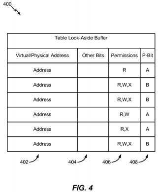
FIG. 5?is a block diagram of a particular illustrative embodiment of a partitioned cache memory?500. The cache memory500?includes a first partition (Partition A)?502?and a second partition (Partition B)?504. The first partition?502?may represent a cache memory area, for example, from address 0xD803 FFFF to 0xD802 0000. The second partition?504?may represent a cache memory area, for example, from address 0xD801 FFFF to 0xD800 0000. In a particular illustrative embodiment, cache replacement
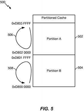
In a particular example, the replacement strategy may be configurable using supervisor control registers, global control registers, or dedicated registers. In a particular example, the global registers may assign a replacement strategy to a particular partition. In another particular example, the global registers may be configured during execution of high priority processes (on the fly) by a particular process to define the replacement strategy for particular partitions.
FIG. 6?is a flow diagram of a particular illustrative embodiment of a method of controlling replacement of items in a partitioned cache memory. The method includes reading a TLB entry to map a virtual address to a physical address and to retrieve a partition indicator associated with a partition of a cache memory that includes at least two partitions, at?602. Advancing to?604, the method includes searching the cache memory for data related to the physical address. At?606, if there is a cache hit, the method advances to?608?and data is retrieved from memory at the physical address. Continuing to610, the method includes outputting the retrieved data. The method terminates at?622.
Returning to?606, if there is a cache miss, the method proceeds to?612?and a cache replacement policy is selected based on the partition indicator. The cache replacement policy may be selected based on a bit setting within a supervisor or global register. Alternatively, a logic circuit may select the policy based on a desired quality of service for a particular process. For example, high quality of service processes may use
Continuing to?614, the method includes retrieving data at the physical address associated with a second memory (such as a main memory). Moving to?616, the method includes identifying a partition of the cache that is associated with the partition indicator. At?618, the method includes selecting a location within the identified partition according to the selected cache replacement policy. Continuing to?620, the method includes replacing the data at the selected location of the identified partition with the retrieved data. The method terminates at?622.
FIG. 7?is a flow diagram of a particular illustrative embodiment of a method of partitioning a cache memory. At?702, the method includes partitioning a cache memory into two or more partitions using a system configuration setting. The system configuration setting defines a size of each of the two or more partitions. Continuing to?704, the method includes configuring a replacement policy associated with each of the two or more partitions. The replacement policy governs replacement access to the cache memory with respect to partitions of the cache memory. In a particular embodiment, the replacement policy can be set by writing replacement policy partition data into at least one of multiple entries in a translation look-aside buffer. The method terminates at?706.
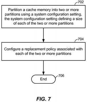
In a particular illustrative embodiment, a first replacement policy is associated with a first partition and a second replacement policy is associated with a second partition of the two or more partitions. In another particular embodiment, a partition is selected and a replacement policy can be invoked on a per application basis. In another particular embodiment, a partition is selected for a particular process and the replacement policy is invoked on a per partition basis. In a particular embodiment, a software process or application may modify the replacement policy during operation. For example, the replacement policy may be modified in response to an application request, in response to an operating system command, or in response to usage information. In a particular example, the replacement policy may be dynamically modified in response to a priority level of a particular process or based on a quality of service indicator or requirement for a particular process. For example, a particular partition and/or a particular replacement policy may be associated with a particular process, based on a determination that such a process is a high priority process. Upon execution of the process, instructions and data associated with the process may be stored in a selected partition and processed using a selected replacement algorithm that corresponds to a desired quality of service.
FIG. 8?is a block diagram of a communications device that includes a partitioned cache memory and a cache replacement control logic circuit. The portable communications device?800?includes a partitioned cache?860, such as the partitioned instruction cache?110?and the partitioned data cache?112?illustrated in?FIG. 1?and such as the cache memory?204?illustrated in?FIG. 2. The portable communications device?800?also includes a cache replacement control logic circuit?870?that is coupled to the partitioned cache?860. The cache replacement control logic circuit?870?may operate similar to the cache control replacement circuitry?104,?224, and?312?of?FIGS. 1-3, respectively. In a particular embodiment, a cache replacement control logic circuit?870?that is coupled to the partitioned cache?860?may include the cache?204, the cache access logic?218, the tag array?220?and the partitioned data cache?228?illustrated in?FIG. 2. The cache replacement control logic circuit?870?may implement at least a portion of one or more of the methods depicted in?FIGS. 6 and 7, such as by selectively controlling replacement of data and instructions within partitions of the partitioned cache?860.
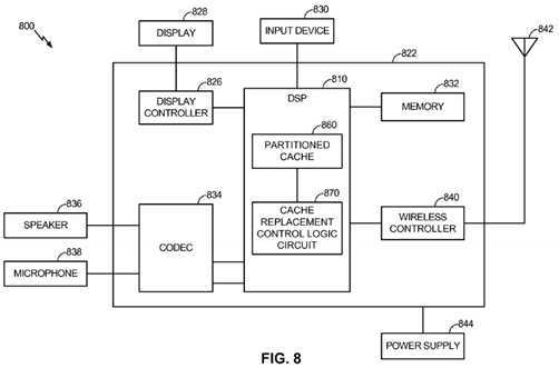
The portable communications device?800?includes an on-chip system?822?that includes a processor, such as a digital signal processor?810. The digital signal processor?810?can include the partitioned cache?860?and the cache replacement control logic circuit?870, as described with respect to?FIGS. 1-3. In a particular illustrative embodiment, the cache replacement control logic circuit?870?and the partitioned cache?860?may be used to control replacement of data within the partitions of the partitioned cache?860?to enhance quality of service to particular threads of a processor, such as the digital signal processor?810.
FIG. 8?also shows a display controller?826?that is coupled to the digital signal processor?810?and to a display?828. Moreover, an input device?830?is coupled to the digital signal processor?810. Additionally, a memory?832?is coupled to the digital signal processor?810. A coder/decoder (CODEC)?834?can also be coupled to the digital signal processor?810. A speaker?836?and a microphone?838?can be coupled to the CODEC?834.
FIG. 8?also indicates that a wireless controller?840?can be coupled to the digital signal processor?810?and to a wireless antenna?842. In a particular embodiment, a power supply?844?is coupled to the on-chip system?822. Moreover, in a particular embodiment, as illustrated in?FIG. 8, the display?828, the input device?830, the speaker?836, the microphone?838, the wireless antenna?842, and the power supply?844?are external to the on-chip system?822. However, each is coupled to a component of the on-chip system?822.
It should be understood that while the cache replacement control logic circuit?870?and the partitioned cache?860?are depicted as separate components of the digital signal processor?810, the cache replacement control logic circuit?870?and the partitioned cache?860?may instead be integrated into a single cache unit, such as the cache?204?illustrated in?FIG. 2. Similarly, it should be understood that multiple cache replacement control logic circuits?870?may be included. Additionally, while the replacement control circuitry has been described with respect to partitioned cache memories, it should be understood that the control strategy may be employed for other types of partitioned memories as well, thereby controlling replacement access to locations within the partitioned memory.
SRC=https://www.google.com.hk/patents/US20100318742
Partitioned Replacement for Cache Memory
标签:des style blog http color io os java ar
原文地址:http://www.cnblogs.com/coryxie/p/3987280.html