标签:disable reserve 配置 ack moni creat inf amp input
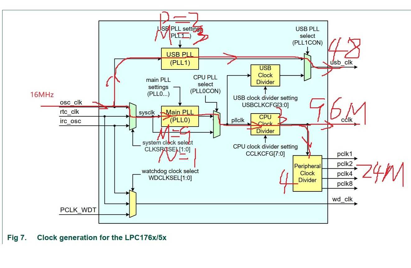
一、时钟的配置路线
二、具体代码实现
1.bsp_clk.c文件中的内容:
/*
 * bsp_clk.c
 *
 *  Created on: 2020年5月20日
 *      Author: Mr.W
 */
#include "bsp_clk.h"
/*
*********************************************************************************************************
*                                             BSP_Init()
*
* Description : Initialize the Board Support Package (BSP).
*
* Argument(s) : none.
*
* Return(s)   : none.
*
* Caller(s)   : Application.
*
* Note(s)     : (1) The PLL0 Frequency is determined by:
*
*                       Fcco = (2 x M x Fin) / N
*
*                       where M   = PLL0 Multipler
*                             N   = PLL0 Pre-dividier
*                            Fin  = PLL0 Input Frequency (Main oscillator).
*
*               (2) PLL0 settings must meet the following:
*                       Fin is in the range of 32Khz to 50 Mhz.
*                       Fcco is in the range of 275 Mhz to 550 Mhz
*
*               (3) The LPC17xx CPU frequency is determined by:
*
*                       CPU_freq = Fcc0 / CPU_Div
*
*               (4) The USB clock frequency is determined by:
*
*                       USB_Clk = M x Fosc, or USB_clk = Fcco / (2 x P)
*
*                       Fcco = Fosc x M x 2 x P, or Fcco = USB_Clk x 2 x P
*
*                       where Fcco = PLL1 output frequency.
*                             M    = PLL1 multiplier.
*                             P    = PLL1 pre-divider.
*                             Fosc = Oscialltor  frequency.
*
*               (5) The PLL1 inputs and settings must meet the following criteria:
*                   Fosc    is in the range of 10 Mhz to 25 Mhz.
*                   USBClk  is 48 Mhz
*                   Fcco    is in the range of 156 Mhz to 320 Mhz
*
*               (6) In this example the LPC1768 operates:
*
*                       PLL0_Fcco = 2 x 9 x 16 / 1
*                       PLL0_Fcco = 288mhz
*
*                       CPU_freq  =  288 Mhz  / 3
*                                 =  96 Mhz
*
*                       PLL1_Fcc0 = 16 x 3 x 2 x 2 = 192 Mhz.
*                       USB_Clk   = 16 x 3         =  48 Mhz.
*********************************************************************************************************
*/
void SystemClk_Init(void)
{
	uint16_t timeout;
	uint32_t ret_val;


	/* [address 0x400FC000-bit15:bit12]Flash加速器配置寄存器,设置Flash的访问时间.
	 * The value of this field plus 1 gives the number of CPU clocks used for a flash access.
	 * 0000	Flash accesses use 1 CPU clock. Use for up to 20 MHz CPU clock.
	 * 0001	Flash accesses use 2 CPU clocks. Use for up to 40 MHz CPU clock.
	 * 0010	Flash accesses use 3 CPU clocks. Use for up to 60 MHz CPU clock.
	 * 0011	Flash accesses use 4 CPU clocks. Use for up to 80 MHz CPU clock.
	 * 0100 Flash accesses use 5 CPU clocks. Use for up to 100 MHz CPU clock.
	 * 0101 Flash accesses use 6 CPU clocks. This “safe” setting will work under any conditions.
	 */
	LPC_SC->FLASHCFG = ((6u - 1u) << 12u | 0x0000003Au);

	/* [address 0x400FC1A0-bit4]系统控制和状态寄存器,设置主振荡器的范围.
	 * 0 The frequency range of the main oscillator is 1 MHz to 20 MHz.
	 * 1 The frequency range of the main oscillator is 15 MHz to 25 MHz.
	 */
	LPC_SC->SCS &= ~(1u << 4u);

	/* [address 0x400FC1A0-bit5]系统控制和状态寄存器,使能主震荡器.
	 * 0 The main oscillator is disabled.
	 * 1 The main oscillator is enabled, and will start up if the correct
	 *	 external circuitry is connected to the XTAL1 and XTAL2 pins.
	 */
	LPC_SC->SCS |= (1u << 5u);

	timeout = 0xFFFFu;
	/* [address 0x400FC1A0-bit6]系统控制和状态寄存器,主震荡寄存器的状态.
	 * 0 The main oscillator is not ready to be used as a clock source.
	 * 1 The main oscillator is ready to be used as a clock source.
	 *   The main oscillator must be enabled via the OSCEN bit.
	 * Wait until the main oscillator is enabled. */
	while(((LPC_SC->SCS & 0x40u) == 0u) && (timeout > 0u))
	{
		timeout--;
	}
	if(timeout <= 0u)
	{
		return;
	}

	/* [address 0x400FC1A8]外设时钟选择寄存器.
	 * 设置所有的外设时钟运行在 CPU_Clk / 4.
	 * 00 PCLK_peripheral = CCLK/4.
	 * 01 PCLK_peripheral = CCLK.
	 * 10 PCLK_peripheral = CCLK/2.
	 * 11 PCLK_peripheral = CCLK/8, except for CAN1, CAN2, and
	 * 	  CAN filtering when “11” selects = CCLK/6.
	 */
	LPC_SC->PCLKSEL0 = 0x00u;
	/* [address 0x400FC1AC]外设时钟选择寄存器. */
	LPC_SC->PCLKSEL1 = 0x00u;

	/* PLL0 values M = PLL0_M & N = PLL0_N. */
	ret_val = ((PLL0_M - 1u) <<  0u)			/* PLL0 Multiplier value. The value stored here is M - 1.
											   	   Supported values for Mare 6 through 512. */
			| ((PLL0_N - 1u) << 16u);			/* PLL0 Pre-Divider value.The value stored here is N - 1.
											   	   Supported values for N are 1 through 32. */

	/* [address 0x400FC088-bit25]PLL0状态寄存器,PLL0连接状态.
	 * This bit reflects the state of the PLLC0 bit in PLL0CON after a valid PLL0 feed.
	 * When PLLC0 and PLLE0 are both one, PLL0 is connected as the clock source for the CPU.
	 * When either PLLC0 or PLLE0 is zero,PLL0 is bypassed.
	 * This bit is automatically cleared when Power-down mode is entered.
	 */
	if(LPC_SC->PLL0STAT & 0x02000000)
	{
		/* [address 0x400FC080-bit1]PLL0控制寄存器,PLL0连接断开.
		 * Disconnect PLL0 with one feed sequence if PLL already connected.
		 */
		LPC_SC->PLL0CON &= ~(1u << 1u);
		/* [address 0x400FC08C-bit7:bit0]Feed寄存器,要想使PLL0CON和PLL0CFG的改变起作用
		 * 必须向PLL0FEED寄存器按顺序写入 0xAA和0x55.
		 * The PLL0 feed sequence must be written to this register in order for
		 * PLL0 configuration and control register changes to take effect.
		 */
		LPC_SC->PLL0FEED = 0x000000AAu;
		LPC_SC->PLL0FEED = 0x00000055u;
	}

	/* [address 0x400FC080-bit0]PLL0控制寄存器,PLL0不使能.
	 * Disable PLL0 with one feed sequence.
	 */
	LPC_SC->PLL0CON &= ~(1u << 0u);
	LPC_SC->PLL0FEED = 0x000000AAu;
	LPC_SC->PLL0FEED = 0x00000055u;

	/* [address 0x400FC104-bit7:bi0]CPU时钟配置寄存器.
	 * 0 pllclk is divided by 1 to produce the CPU clock. This setting is
	 *   not allowed when the PLL0 is connected, because the rate would always
	 *   be greater than the maximum allowed CPU clock.
	 * 1 pllclk is divided by 2 to produce the CPU clock. This setting is
	 *   not allowed when the PLL0 is connected, because the rate would always
	 *   be greater than the maximum allowed CPU clock.
	 * 2 pllclk is divided by 3 to produce the CPU clock.
	 * 3 pllclk is divided by 4 to produce the CPU clock.
	 * ...
	 * 255 pllclk is divided by 256 to produce the CPU clock.
	 *
	 * Change the CPU clock divider setting to speed operation without PLL0.
	 */
	LPC_SC->CCLKCFG = (1u - 1u);

	/* [address 0x400FC10C-bit1:bit0]时钟源选择寄存器.
	 * 00 Selects the Internal RC oscillator as the PLL0 clock source(default).
	 * 01 Selects the main oscillator as the PLL0 clock source.
	 * 10 Selects the RTC oscillator as the PLL0 clock source.
	 * 11 Reserved, do not use this setting.
	 *
	 *  Select the main osc. as the PLL0 clock source.
	 */
	LPC_SC->CLKSRCSEL = 0x01u;

	/* [address 0x400FC084]PLL0配置寄存器.
	 * bit14:bit0 PLL0 Multiplier value.
	 * bit23:bit16 PLL0 Pre-Divider value.
	 * Write to the PLLCFG and make it effective with one one feed sequence.
	 */
	LPC_SC->PLL0CFG = ret_val;
	LPC_SC->PLL0FEED = 0x000000AAu;
	LPC_SC->PLL0FEED = 0x00000055u;

	/* [address 0x400FC080-bit0]PLL0控制寄存器,PLL0使能.
	 * Enable PLL0 with one feed sequence.
	 */
	LPC_SC->PLL0CON |= (1u << 0u);
	LPC_SC->PLL0FEED = 0x000000AAu;
	LPC_SC->PLL0FEED = 0x00000055u;

	/* [address 0x400FC104-bit7:bi0]CPU时钟配置寄存器.
	 * 0 pllclk is divided by 1 to produce the CPU clock. This setting is
	 *   not allowed when the PLL0 is connected, because the rate would always
	 *   be greater than the maximum allowed CPU clock.
	 * 1 pllclk is divided by 2 to produce the CPU clock. This setting is
	 *   not allowed when the PLL0 is connected, because the rate would always
	 *   be greater than the maximum allowed CPU clock.
	 * 2 pllclk is divided by 3 to produce the CPU clock.
	 * 3 pllclk is divided by 4 to produce the CPU clock.
	 * ...
	 * 255 pllclk is divided by 256 to produce the CPU clock.
	 *
	 * Change the CPU clock divider setting for operation with PLL0.
	 */
	LPC_SC->CCLKCFG = (CPU_DIV - 1u);

	timeout = 0xFFFF;
	/* [address 0x400FC088-bit26]PLL0状态寄存器,反应PLL0锁状态.
	 * 0 PLL0 is not locked.
	 * 1 PLL0 is locked onto the requested frequency.
	 *
	 * Wait for PLL0 to achieve lock by monitoring the PLOCK0 bit in the PLL0STAT.
	 */
	while(((LPC_SC->PLL0STAT & 0x04000000u) == 0u) && (timeout > 0u))
	{
		timeout--;
	}
	if(timeout == 0u)
	{
		return;
	}

	/* [address 0x400FC080-bit1]PLL0控制寄存器,PLL0连接.
	 * Connect PLL0 with one feed sequence.
	 */
	LPC_SC->PLL0CON |= (1u << 1u);
	LPC_SC->PLL0FEED = 0x000000AAu;
	LPC_SC->PLL0FEED = 0x00000055u;

#if USBCLK_EN
	/* PLL1 values M = PLL1_M & PLL1_P = 2. */
	ret_val = ((PLL1_M - 1u) << 0u)			/* PLL1 Multiplier value. The value stored here is M - 1.
										   	   Supported values for Mare 6 through 512. */
			| ((PLL1_P - 1u) << 5u);		/* PLL1 Pre-Divider value.The value stored here is N - 1.
										   	   Supported values for N are 1 through 32. */
	/* [address 0x400FC0A0-bit1]PLL1控制寄存器,PLL1连接断开.
	 * Disconnect PLL1 with one feed sequence.
	 */
	LPC_SC->PLL1CON &= ~(1u << 1u);
	LPC_SC->PLL1FEED = 0x000000AAu;
	LPC_SC->PLL1FEED = 0x00000055u;

	/* [address 0x400FC0A0-bit0]PLL1控制寄存器,PLL1不使能.
	 * Disable PLL1 with one feed sequence  */
	LPC_SC->PLL1CON &= ~(1u << 0u);
	LPC_SC->PLL1FEED = 0x000000AAu;
	LPC_SC->PLL1FEED = 0x00000055u;

	/* [address 0x400FC0A4]PLL1配置寄存器.
	 * bit4:bit0 PLL1 Multiplier value.
	 * bit6:bit5 PLL1 Divider value.
	 * Write to the PLLCFG and make it effective with one one feed sequence.
	 */
	LPC_SC->PLL1CFG = ret_val;
	LPC_SC->PLL1FEED = 0x000000AAu;
	LPC_SC->PLL1FEED = 0x00000055u;

	/* [address 0x400FC0A0]PLL1控制寄存器,PLL1使能.
	 * Enable PLL1 with one feed sequence. */
	LPC_SC->PLL1CON |= (1u << 0u);
	LPC_SC->PLL1FEED = 0x000000AAu;
	LPC_SC->PLL1FEED = 0x00000055u;

	timeout = 0xFFFF;
	/* [address 0x400FC0A8-bit10]PLL1状态寄存器,反应PLL1锁状态.
	 * 0 PLL1 is not locked.
	 * 1 PLL1 is locked onto the requested frequency.
	 *
	 * Wait for PLL1 to achieve lock by monitoring the PLOCK1 bit in the PLL1STAT.
	 */
	while(((LPC_SC->PLL1STAT & 0x0400u) == 0u) && (timeout > 0u))
	{
		timeout--;
	}
	if(timeout == 0u)
	{
		return;
	}

	/* [address 0x400FC0A0]PLL1控制寄存器,PLL1连接.
	 * Connect PLL1 with one feed sequence
	 */
	LPC_SC->PLL1CON |= (1u << 1u);
	LPC_SC->PLL1FEED = 0x000000AAu;
	LPC_SC->PLL1FEED = 0x00000055u;
#endif

	/* Set 6 cycles to acces the Flash memory. */
	LPC_SC->FLASHCFG = ((6u - 1u) << 12u | 0x0000003Au);
}
2.bsp_clk.h文件中的内容:
/*
 * bsp_clk.h
 *
 *  Created on: 2020年5月20日
 *      Author: Mr.W
 */

#ifndef BSP_CLK_H_
#define BSP_CLK_H_

#include "LPC17xx.h"

#define USBCLK_EN				0						/* 控制USB时钟配置 */


#define PLL0_M					9u						/* PLL0倍频值,取值范围6-512 */
#define PLL0_N					1u						/* PLL0分频值,取值范围1-32 */

#if USBCLK_EN
#define PLL1_M					3u						/* PLL1倍频值,取值范围1-32 */
#define PLL1_P					2u						/* PLL1分频值,取值范围1-8 */
#endif
#define CPU_DIV					3u						/* CPU时钟分频,取值范围0-255 */

#define FOSC					16000000u				/* 振荡器频率16MHz */
#define FCCO					((2u * PLL0_M * FOSC)/PLL0_N)
#define CPU_CLK					FCCO/CPU_DIV			/* CPU时钟 */

void SystemClk_Init();

#endif /* BSP_CLK_H_ */
标签:disable reserve 配置 ack moni creat inf amp input
原文地址:https://www.cnblogs.com/wenhao-Web/p/12925622.html