标签:des blog http io ar os sp for on


Synchronous buck regulators offer high efficiency and are popular in applications in which available input voltages are 12V or less. However, as input voltage approaches 100V, wide-range-regulator design becomes more difficult, and the choice of suitable ICs narrows considerably. This Design Idea combines a current-mode PWM IC for flyback-regulator circuits with a 100V gate-driver IC to produce a relatively high-performance synchronous buck regulator that can operate at inputs as high as 100V.
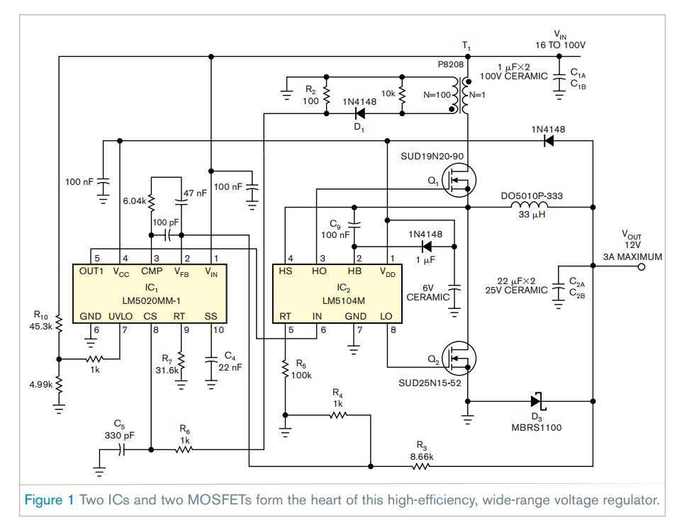
The circuit in Figure 1 uses National Semiconductor‘s LM5020 current-mode PWM, IC1, to drive an LM5104 gate driver, IC2, forming a synchronous controller. The LM5020 contains an internal linear regulator that accepts input as high as 100V and can also deliver an output that can supply drive current to the LM5104. To reduce power dissipation at high input voltages, after initial power application, diode D2, a 1N4148, supplies an 11.5V bootstrap voltage to the remainder of the circuit. Transformer T1, a 100-to-1 current transformer from Pulse Engineering, provides current feedback during MOSFET Q1‘s on-time. Q1 and Q2 are Siliconix Dpak devices, which have low gate-charge requirements and low on-resistances to minimize total switching losses at the circuit‘s 200-kHz operating frequency. All capacitors are of ceramic-dielectric construction to withstand high temperature and to meet packaging-size constraints.
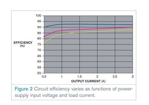
For sustained operation at high input voltage, maximum current, and elevated-temperature conditions, transistor Q1 requires an adequate heat sink or cooling airflow to maintain its junction temperature below the 175°C maximum specification. Q1 has a low junction-to-case thermal resistance, and thus its case temperature must not exceed 160°C. L1, the model DO5010 unshielded ferrite-core inductor from Coilcraft, presents a small pc-board footprint and offers a high saturation-current rating but represents this design‘s dominant loss component. For applications with less critical space requirements, you can improve circuit efficiency by increasing L1‘s inductance and size, thus reducing ripple current and enabling use of a larger core and increased winding-wire gauge. Reducing the output voltage improves efficiency, but, as output voltage drops below the circuit‘s 8V bootstrap voltage, IC1 dissipates additional power and requires caution to avoid exceeding its ratings. Figure 2 shows the circuit‘s measured efficiency versus output current for three input voltages.
One practical application for the circuit met a customer‘s requirement for a dc/dc converter that would operate from a 24V source and deliver 12V output at currents as high as 3A. This routine-sounding specification also requires operation in a physically and electrically harsh environment in which the packaged circuit resides on an engine block that reaches a temperature of 125°C, and ambient-air temperature reaches 100°C. In addition, the power source comprises two series-connected 12V batteries that provide a nominal voltage of 24V, which in practice varies from 18 to 40V and includes inductively induced load-dump voltage spikes that reach 100V.
Wide-range regulator delivers 12V, 3A output from 16 to 100V source
标签:des blog http io ar os sp for on
原文地址:http://www.cnblogs.com/shangdawei/p/4128247.html