标签:blog http io ar os sp for on div
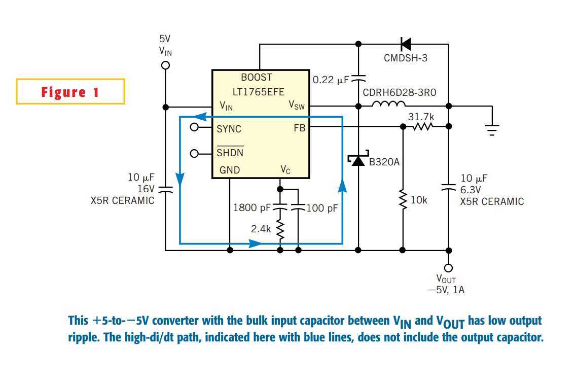
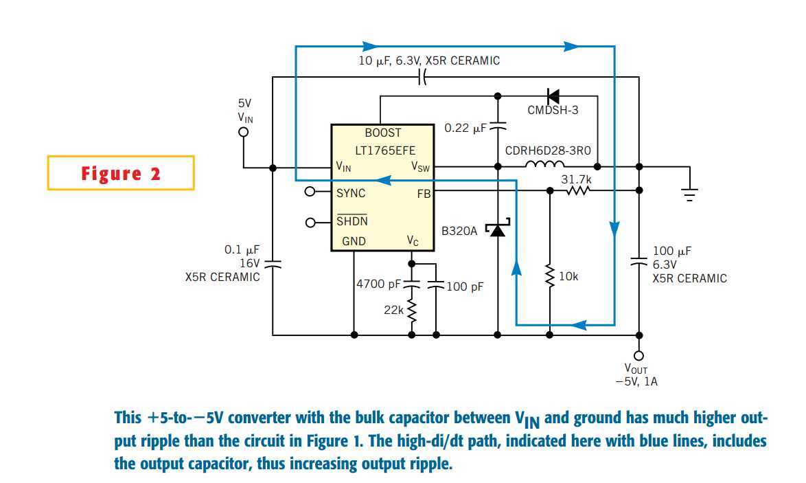
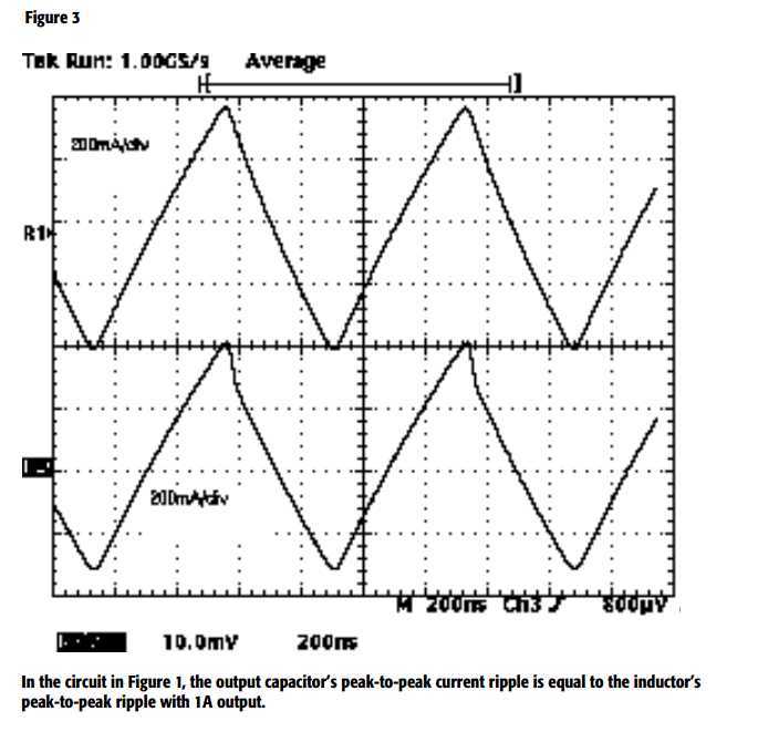
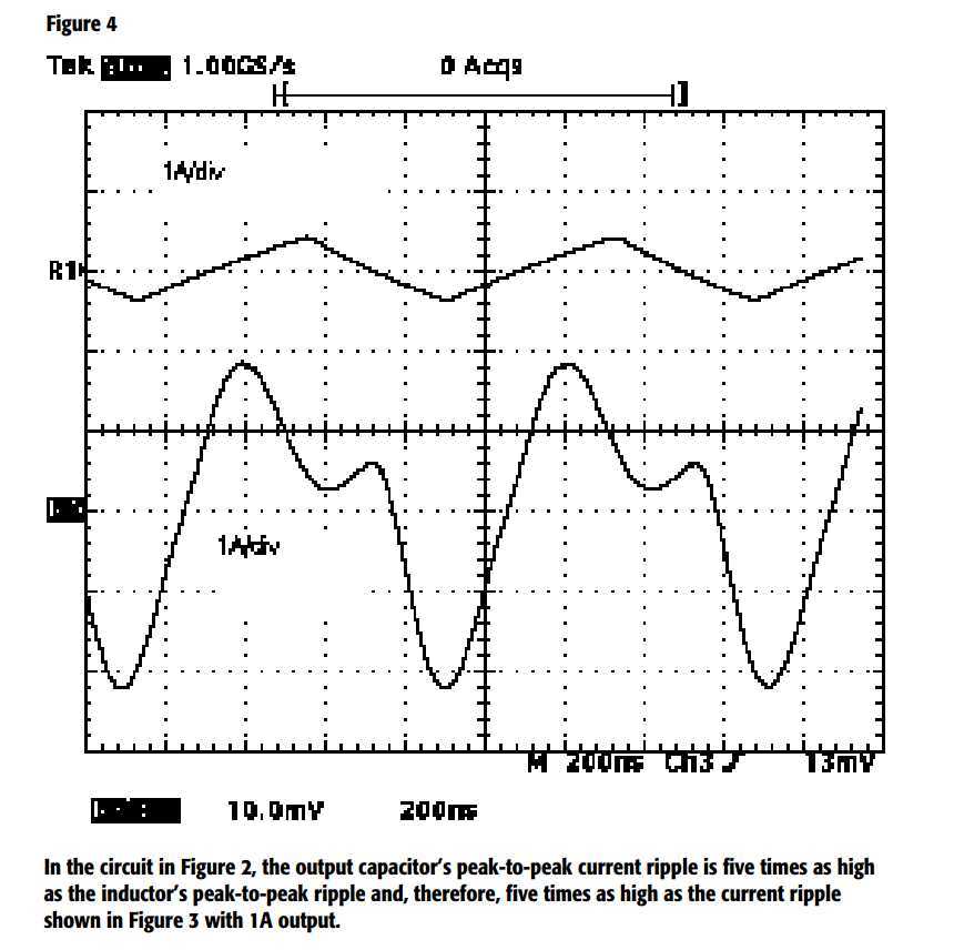
Low-ripple-voltage positive-to-negative dc/dc converters find use in many of today‘s high- frequency and noise-sensitive disk drives, battery-powered devices, portable computers, and automotive applications. Like a positive buck converter, a positive-to-negative converter can have low output-ripple voltage if you place the bulk input capacitor between VIN and VOUT rather than between VIN and ground. A common misconception is that positive-to-negative converters in the first configuration have noisy outputs. This configuration actually solves noise problems rather than introducing them. In either configuration, the VIN and ground pins of the IC connect to VIN and VOUT, respectively (Figure 1 and Figure 2). Therefore, placing the input capacitor between VIN and VOUT is equivalent to placing it between the IC‘s VIN and ground pins (Figure 1). The other, commonly accepted method of placing the bulk input capacitor between VIN and ground (Figure 2) significantly increases the output-voltage ripple (Figure 3 and Figure 4). To make matters worse, this configuration requires an additional high-frequency bypass capacitor between the VIN and ground pins of the IC.
In simple positive-to-negative converters, such as those in Figure 1 and Figure 2, the output-voltage ripple is
ΔVOUT(P-P)=ESRCOUT×ΔICOUT(P-P).
Low-ESR output capacitors, such as ceramics, help to minimize the output-voltage ripple in dc/dc converters. For a given output-capacitor ESR, you can further reduce the output-voltage ripple by minimizing the current ripple that the output capacitor is forced to absorb. In Figure 2, the output capacitor is part of the high-di/dt switching-current path, making the output voltage ripple proportionately larger. With the bulk input capacitor placed as shown in Figure 1, the peak-to-peak ripple current in the output capacitor is equal to the peak-to-peak ripple current in the inductor:
ΔICOUT(P-P)=ΔIL(P-P)=(VIN×duty cycle)/(fSW×L), where ΔICOUT(P-P)=output ripple current, ΔIL(P-P)=inductor ripple current, and fSW=switching frequency.
When the bulk input capacitor is placed as shown in Figure 2, the peak-to-peak ripple current in the output capacitor is much higher than the inductor‘s ripple current alone; it is almost equal to the inductor‘s ripple current plus the input capacitor‘s ripple current:
ΔICIN(P-P)=IL(P)=IOUT+IIN+ΔIL(P-P)/2, and ΔICOUT (P-P)~ΔIL(P-P)+ΔICIN(P-P). With much lower output-capacitor ripple current, the output capacitor in the circuit in Figure 1can be much smaller than that of the circuit in Figure 2. Also, it needs to handle much less rms ripple current (approximately equal to peak-to-peak ripple current divided by the square root of 12). Another advantage of removing the output capacitor from the high-di/dt switching loop (by judicious placement of the input capacitor) is a greatly simplified layout. You must place the high-di/dt components in Figure 1 in the smallest loop possible to minimize trace inductance and the resulting voltage (noise) spikes. With one fewer component to worry about in the layout, you can more easily create a noise-free circuit using the layout in Figure 1 than it is using the one inFigure 2.


Lower dc/dc-converter ripple by using optimum capacitor hookup
标签:blog http io ar os sp for on div
原文地址:http://www.cnblogs.com/shangdawei/p/4128298.html