标签:des style blog http io ar color os sp
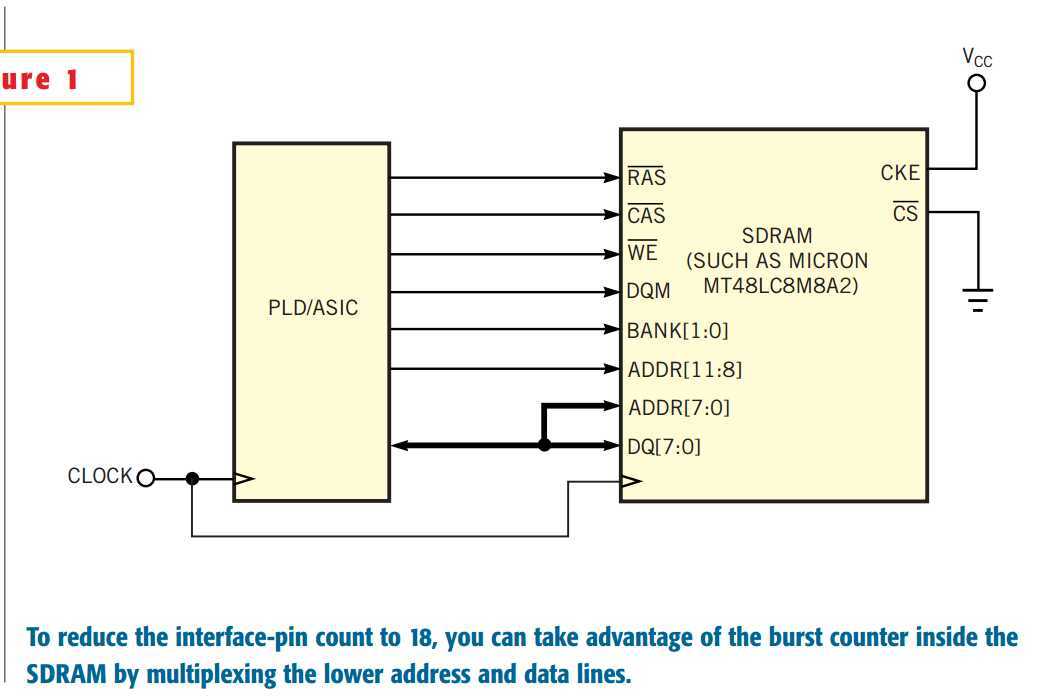
Many designs need deep buffering but don‘t require ultrahigh-memory bandwidth. Examples include image and audio processing, as well as some deep-FIFO applications. These designs often use a single ×8 SDRAM device that connects to an FPGA or ASIC. This approach solves the buffering problem but also burns a lot of valuable pins, which can be as many as 27 for a single SDRAM device. The design inFigure 1 takes advantage of the burst counter inside the SDRAM to reduce this pin count to 18 by multiplexing the lower eight address lines with the data. The efficiency loss is low; the design requires only one extra clock during the write burst. Figure 1uses an 8Mx8, 125-MHz SDRAM, but this technique works with any SDRAM.
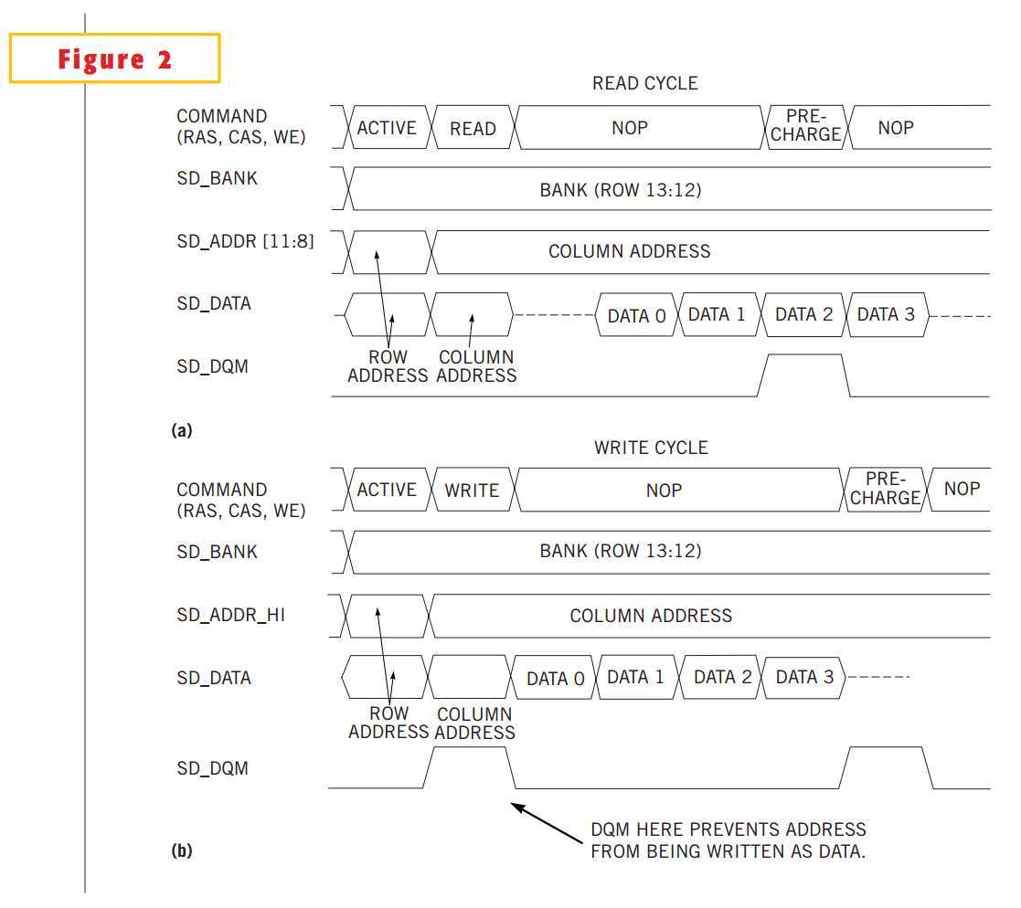
The read- and write-cycle timing diagrams reveal the secret (Figure 2). The figureshows a burst of 4, but any power-of-2 burst works. These diagrams assume a 50-MHz system clock, a read latency of 2, and a full-page burst. During the read cycle (Figure 2a), the data bus is inactive during the initial portion of the cycle (when the row and column addresses are presented), so there‘s no problem with using the data bus to carry address data. A precharge command ends the burst and prepares the RAM for the next access.
For the write cycle, however, some trickery is necessary (Figure 2b). Normally, the first byte of write data is presented to the SDRAM with the Write command, along with the starting column address for that burst. By asserting the DQM (data-mask) signal, the SDRAM ignores the data lines during this phase, thus allowing them to be used for the column address.
Note that the DQM signal does not prevent the internal column address from incrementing, however. Thus, the write-column address presented with the Write command must be one less than the desired burst starting address. For FIFO designs, this requirement is trivial because you can initialize the write-address column counter to –1 rather than 0. The column-address counter in the SDRAM wraps around at the end of the column, so this approach works even at the beginning of a column.
You can download a simplified version of a FIFO controller that uses this technique, described in the Verilog language. The listing omits some of the details, such as SDRAM refresh/init cycles, and FIFO flags, to highlight the portions relevant to this design. This controller uses a simple eight-state finite-state machine to generate the SDRAM control signals and uses a pair of row/column counters to keep track of the FIFO put/get pointers. The special initialization and incrementing of the write row and column pointers satisfies the requirement that the write column start off one behind the desired write address. The code occupies 35% of a small Xilinx SpartanXL-S10 device, and runs at 50 MHz. For the sake of example, all of the outputs are combinatorial, but a true high-speed design should use registered I/O.
You can extend this idea to ×16 SDRAMs and to multiplex a few more of the address lines while getting a boost in memory bandwidth. If you do extend the idea, be careful with SDRAM line A10 because this line has special meaning during some SDRAM commands. You can also use this technique with double-data-rate SDRAMs.


;*********************************************************************************
; di2659.txt
;
; LISTING 1 - FIFO CONTROLLER
;
; "SDRAM interface slashes pin count," EDN, March 29, 2001, pg 132
; http://www.ednmag.com/ednmag/reg/2001/03292001/designideas.htm#07di4
;*********************************************************************************

`timescale 1 ns / 1 ns

/*
** Minimal-pin SDRAM controller with FIFO address counters.  This
** has a simple do_write/wr_ok, do_read/rd_ok handshake for data input &
** output.  The ‘rst_fifo‘ signal syncronously resets the fifo
**
** Author: Tim Hellman, M&M Consulting
*/
module sdctl(clk, reset_,

        rst_fifo, do_write, do_read, wr_data_in,   /* Fifo I/O */
        wr_ok, rd_ok, rd_data_out,

        sd_ras_, sd_cas_, sd_we_, sd_dqm, sd_bank,  /* SDRAM signals */
        sd_addr_hi, sd_data
        );

 input clk, reset_, do_write, do_read, rst_fifo;
 input [7:0] wr_data_in;

 output wr_ok, rd_ok, sd_ras_, sd_cas_, sd_we_, sd_dqm;
 output [7:0] rd_data_out;
 output [1:0] sd_bank;
 output [11:8] sd_addr_hi;

 inout [7:0] sd_data;

 /*
 ** States
 */
 parameter StIdle = 0, StActive = 1, StRdWr = 2, StData1 = 3,
       StData2 = 4, StData3 = 5, StRdPrech = 6, StWrPrech = 7;

 reg [2:0] State;
 reg [13:0] RdRow, WrRow;
 reg [8:2] RdCol, WrCol;
 reg sd_data_ena, doing_write;

 always @(posedge clk or negedge reset_)
   if (!reset_) begin
     RdRow <= 0;  WrRow <= 0; RdCol <= 0; WrCol <= 7‘h7f;
     sd_data_ena <= 0; State <= StIdle; doing_write <= 0;
   end
   else begin

     /*
     ** State machine.  Once kicked off, run through all states
     */
     if (State == StIdle && (do_write | do_read)) begin
        doing_write <= #1 do_write;
        State <= #1 State + 1;
     end
     else if (State != StIdle) State <= #1 State + 1;

     /*
     ** Read/write counters (note that write col counter starts
     ** one behind read).  The Write row also increments when
     ** WrCol == ‘7e (because WrCol is always one behind)
     */
     if (rst_fifo) {RdRow,RdCol} <= #1 0;
     else if (State == StWrPrech && !doing_write)
                  {RdRow,RdCol} <= #1 {RdRow,RdCol} + 1;

     if (rst_fifo) WrCol <= #1 7‘h7f;
     else if (State == StWrPrech && doing_write) WrCol <= #1 WrCol + 1;

     if (rst_fifo) WrRow <= #1 0;
     else if (State == StWrPrech && doing_write && WrCol == 7‘h7e)
                WrRow <= #1 WrRow + 1;

     if (State == StIdle && (do_read | do_write)) sd_data_ena <= #1 1;
     else if (doing_write && (State == StRdPrech)
          || !doing_write && (State == StRdWr))   sd_data_ena <= #1 0;

   end

   /*
   ** Generate the SDRAM ‘command‘ bits (combinatorially)
   */
   reg [2:0] SdCmd;
   always @(State or doing_write) begin
     case (State)
       StActive: SdCmd = 3;
       StRdWr: SdCmd = doing_write ? 4 : 5;
       StRdPrech: SdCmd = doing_write ? 7 : 2;
       StWrPrech: SdCmd = doing_write ? 2 : 7;
       default: SdCmd = 7;  // NOP
     endcase
   end
   assign {sd_ras_, sd_cas_, sd_we_} = SdCmd;

   /*
   ** Data output is either address or data
   */
   wire [8:0] ColAddr  = doing_write ? {WrCol, 2‘b11} : {RdCol, 2‘b00};
   wire [13:0] RowAddr = doing_write ? WrRow : RdRow;

   assign wr_ok = (State >= StData1 && State <= StRdPrech) &  doing_write;
   assign rd_ok = (State >= StData2 && State <= StWrPrech) & !doing_write;

   /* Upper bits of column. address must equal 0 */
   wire [11:0] MuxAddr = (State == StActive) ? RowAddr : {3‘b0,ColAddr};

   assign sd_bank = RowAddr[13:12];
   assign sd_addr_hi = MuxAddr[11:8];
   wire [7:0] DataOut = (State == StActive || State == StRdWr) ?
             MuxAddr[7:0] : wr_data_in;

   assign sd_data = sd_data_ena ? DataOut : ‘hz;
   assign rd_data_out = sd_data;

   assign sd_dqm = doing_write ? (State == StRdWr | State == StWrPrech) :
                                 (State == StRdPrech);

endmodule
SDRAM interface slashes pin count
标签:des style blog http io ar color os sp
原文地址:http://www.cnblogs.com/shangdawei/p/4128501.html