标签:blog http io ar os sp for strong on
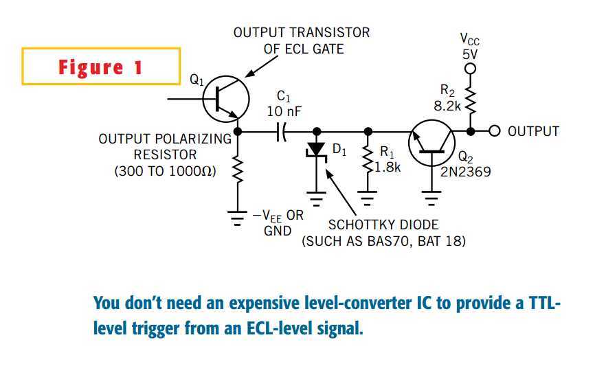
ECL circuits typically have relatively small logic spans of approximately 800 mV. Because of the small span, to drive TTL circuits from ECL levels normally entails the use of level converters, such as the MC10125, or comparators. Such circuits are relatively power-hungry and expensive. However, they are sometimes simply unnecessary. The circuit in Figure 1 allows you to trigger some TTL circuitry by generating a fairly short negative-going pulse from the trailing edge of the ECL signal. The main requirement for the circuit to work is that the rate of ECL signal be in the tens of kilohertz. Such signals sometimes appear at the rear panels of some older types of measurement equipment. Such equipment can include sampling oscilloscopes or time-domain reflectometers, such as the 7S12 or 7S14 from Tektronix. In a measurement setup, the circuit in Figure 1 exploits the sampling gate from a 7S12 plug-in unit.
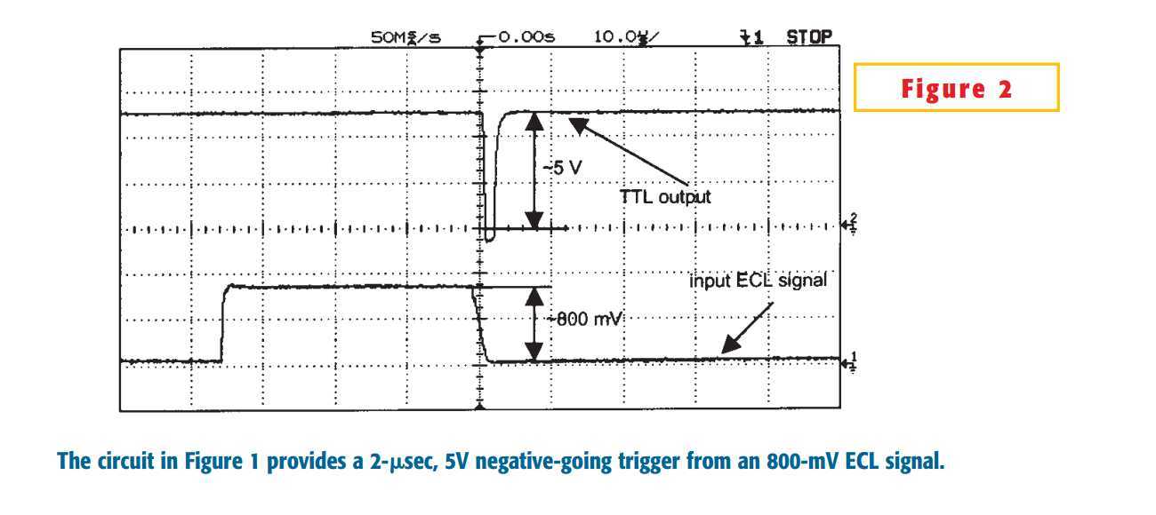
Figure 2 shows the waveforms associated with the circuit in Figure 1. The positive portion of the ECL signal charges capacitor C1 through the Schottky diode, D1. In this part of the operating cycle, transistor Q2 is off, and the output voltage is approximately 5V. On the negative-going edge of the driving pulse, the charge from coupling capacitor C1 causes the base-emitter junction of Q2 to conduct, driving the transistor into saturation. The output voltage assumes a level slightly below 0V. The duration of the generated negative-going pulse depends on the speed with which C2discharges. The discharge takes place through the base-emitter junctions of Q1 and Q2and resistor R1. The duration is difficult to calculate, but for a rough estimate, you can use the following equation:

where ΔV≈0.8V is the ECL span, VDS≈0.15V is the voltage drop of the Schottky diode, and VBE≈0.6V is the voltage drop of the base-emitter junctions. In practice, the durations are shorter than predicted because the equation does not take account of the base-emitter resistances of Q1 and Q2. For the components in Figure 1, the duration is approximately 2 µsec. The crucial component in the circuit is D1, which must be a Schottky type, because of the voltage swing of the ECL signal, which is nearly the same as the base-emitter voltage of the conducting silicon transistor. Proper operation of the circuit occurs because of the voltage difference between Schottky and silicon-junction levels, which is typically 0.1 to 0.3V. This difference allows for the strong saturation of Q2 just after the trailing edge of the ECL signal.


Trigger a TTL circuit from ECL levels
标签:blog http io ar os sp for strong on
原文地址:http://www.cnblogs.com/shangdawei/p/4128381.html