标签:des blog http io ar os sp for on
The achievable accuracy for systems with multiple ADCs depends directly on the reference voltages applied to the ADCs. Medical-ultrasound-imaging systems, for example, commonly include a large number of ADCs in the system‘s beam-former electronics, with the ADCs usually organized in groups of 16, 24, 32, and so on. To obtain maximum beam accuracy, you must minimize errors in the ADC path. Poor accuracy of the reference voltages of the individual ADCs degrades the overall system accuracy. Another source of degradation is the distributed load, which comprises many individual resistive and capacitive loads. Several approaches are available to provide the reference voltage for such ADC arrays:
Individual on-chip references. Though this approach offers a convenient local connection to each ADC, it can result in relatively poor matching among the converters.
A single external reference voltage applied to all ADC reference inputs. Such a configuration allows you to engineer an external reference voltage of arbitrary accuracy but incurs errors from the small variations among the internal ladders of the ADCs.
An external reference directly driving the ADCs‘reference-ladder taps. This option delivers maximum gain accuracy by directly controlling the reference voltage applied to each ADC ladder. However, it requires driving the relatively low resistance of the ladders. Moreover, some ADCs do not allow access to that internal bias point.
In many applications, gain and noise level have a major effect on ADC accuracy. The gain of an ADC is in effect the slope of its transfer function, which relates analog inputs to the allowable range of digital-output codes. One way to quantify gain is to measure the full-scale input range, which is a direct function of the reference-voltage level. For medical- ultrasound-imaging systems, variations in the full-scale ranges of the ADCs can cause errors in beam formation. The variations also affect the ADCs‘ clipping point—an effect that may be important is certain signal-demodulation schemes. An ADC‘s noise level determines its usable dynamic range. This dynamic range should be as great as possible. The reference-noise component of ADC noise can be additive or multiplicative. Local bypass capacitors on the individual ADCs can easily filter additive noise. Multiplicative noise, on the other hand, is more insidious. For ultrasound applications, reference noise in the audio-frequency spectrum can modulate large "stationary" signals in the RF spectrum. Such signals arise from stationary tissue in the ultrasound target.
Audio modulation produces sidebands in the RF signal that a Doppler detector can demodulate, producing audio tones. To estimate the amount of audio noise tolerable in an ultrasound application, assume a nearly full-scale RF signal applied to a 10-bit ADC such as the MAX1448. The device‘s dynamic range of almost 60 dB equates to a noise floor of –60 dBFS (relative to full-scale). You can normalize that noise level to a 1-Hz bandwidth. The Nyquist bandwidth for an 80-MHz sampling rate is 40 MHz. The correction factor is ![]() =76 dB, which places the ADC‘s noise floor at –60 dBFS–76 dBFS=–136 dBFS. Because a conservative design requires the reference-voltage noise to be at least 20 dB lower (–156 dBFS), a 2V reference requires an extremely low noise level of 33 nV p-p (approximately 8 nV/
=76 dB, which places the ADC‘s noise floor at –60 dBFS–76 dBFS=–136 dBFS. Because a conservative design requires the reference-voltage noise to be at least 20 dB lower (–156 dBFS), a 2V reference requires an extremely low noise level of 33 nV p-p (approximately 8 nV/![]() ).
).
A multiple-ADC array may require a more accurate reference voltage than the one internal to each converter. The reference voltage internal to MAX144x converters, for example, has an accuracy of ±1%. The following two circuits are reference designs for such arrays. They feature a single, common low-frequency noise filter, and they offer high-frequency noise suppression via local decoupling capacitors connected to individual ADCs.
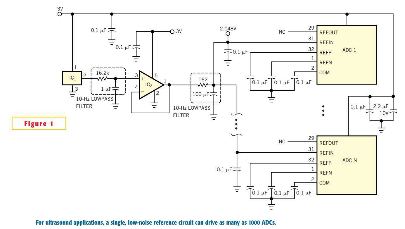
Multiple-converter systems based on the MAX144x family are well-suited for use with a common reference voltage. You can the REFIN pin of these converters to an external reference source and thus eliminate the need for any circuit modification. Moreover, the high input impedance of REFIN (even of multiple REFIN terminals connected in parallel) results in only a small load-current drain. Figure 1 shows a precision source, such as the MAX6062, that generates an external dc level of 2.048V and exhibits a noise-voltage density of 150 nV/![]() . The output of the IC passes through a one-pole lowpass filter with 10-Hz cutoff frequency to op amp IC2, which buffers the reference. The buffered reference voltage then passes through a second 10-Hz lowpass filter. IC2exhibits a low offset voltage for high gain accuracy and a low noise level. The passive 10-Hz filter following the buffer attenuates noise produced in the voltage-reference IC and buffer stage. The filtered noise density, which decreases with frequency, meets the noise levels required for precision-ADC operation.
. The output of the IC passes through a one-pole lowpass filter with 10-Hz cutoff frequency to op amp IC2, which buffers the reference. The buffered reference voltage then passes through a second 10-Hz lowpass filter. IC2exhibits a low offset voltage for high gain accuracy and a low noise level. The passive 10-Hz filter following the buffer attenuates noise produced in the voltage-reference IC and buffer stage. The filtered noise density, which decreases with frequency, meets the noise levels required for precision-ADC operation.
Converters of the MAX144x family specify a typical gain error of ±4.4% (better than ±0.5 dB). This performance is better than the gain tolerance of all other building blocks in the signal path of an ultrasound receiver. Note that the circuit in Figure 1ensures proper power-up/power-down sequencing, because all active parts receive their power from the same supply-voltage rail. This approach yields excellent gain matching and an extremely low noise level with minimal circuitry. The circuit should prove adequate in many applications that require multiple gain-matched ADCs.
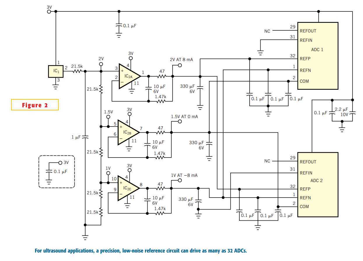
For applications requiring more stringent gain matching, the MAX144x family fills the bill. In Figure 2, connecting each REFIN to analog ground disables the internal reference of each device. You can thus directly drive the internal reference ladders from a set of external reference sources. These voltages can have an arbitrarily tight tolerance; the ADCs typically track them within 0.1%. ADCs of this family have 4-kΩ resistance across the ladder‘s reference connection, so it‘s easy for the reference source to drive the load, even with many ADCs connected in parallel. IC1 generates a dc level of 2.500V, followed by a 10-Hz lowpass filter and a precision voltage divider. The buffered outputs of this divider provide 2, 1.5, and 1V, with an accuracy that depends on the tolerances of the divider resistors. The quad op amp IC2, selected for its low noise and dc offset, buffers the three voltages.
The individual voltage followers connect to 10-Hz lowpass filters, which filter both the reference-voltage and buffer-amplifier noise to a level of 3 nV/![]() . The 2 and 1V reference voltages set the differential full-scale range of the associated ADCs at 2V p-p. The 2 and 1V buffers drive the ADCs‘ internal ladder resistances between them. The load is 4 kΩ divided by the number of ADCs in the circuit. As an example, 32 ADCs draw 8 mA from the supplies, a load current that is well within the capability of IC2. The gain accuracy of the configuration in Figure 2 can be almost arbitrarily tight, depending on the accuracy grade of IC1 and the tolerances of the resistors in the voltage divider. The gain matching of the ADCs in such a configuration is typically 0.1%. With a noise level below 3 nV/
. The 2 and 1V reference voltages set the differential full-scale range of the associated ADCs at 2V p-p. The 2 and 1V buffers drive the ADCs‘ internal ladder resistances between them. The load is 4 kΩ divided by the number of ADCs in the circuit. As an example, 32 ADCs draw 8 mA from the supplies, a load current that is well within the capability of IC2. The gain accuracy of the configuration in Figure 2 can be almost arbitrarily tight, depending on the accuracy grade of IC1 and the tolerances of the resistors in the voltage divider. The gain matching of the ADCs in such a configuration is typically 0.1%. With a noise level below 3 nV/ at 100 Hz, this circuit provides exemplary performance. As in Figure 1, the common power supply for all active components removes any concern about power-supply sequencing.


Circuit provides reference for multiple ADCs
标签:des blog http io ar os sp for on
原文地址:http://www.cnblogs.com/shangdawei/p/4128390.html