标签:des blog http io ar os sp for strong
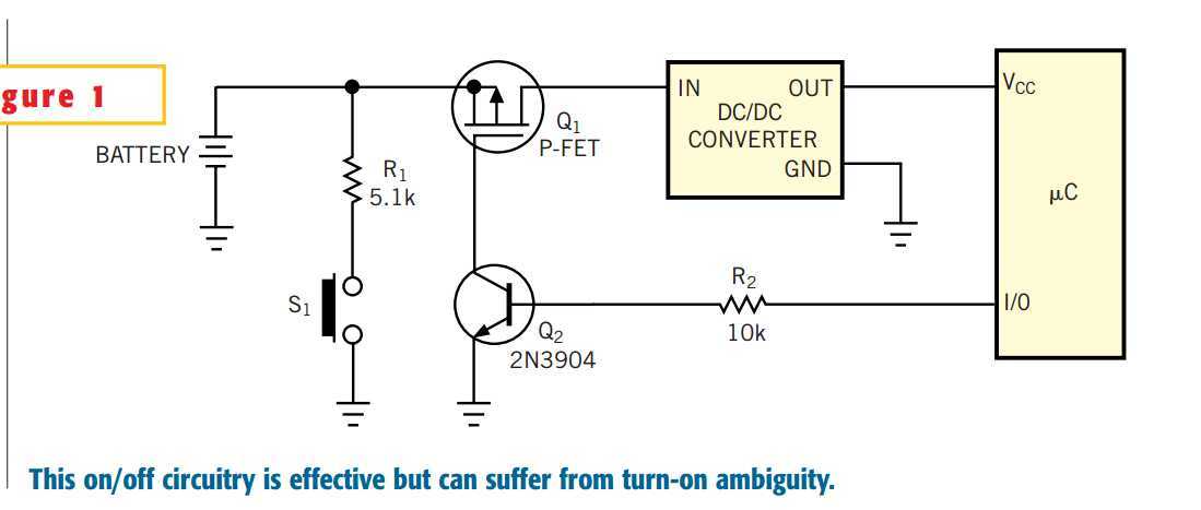
Figure 1 shows an example of on/off circuitry commonly used in battery-operated devices. The p-channel MOSFET, Q1, serves as a power switch. When you push the On button, S1, Q1‘s gate goes low. Q1 turns on and supplies battery voltage to the dc/dc converter. Depending on the battery voltage in the device, the dc/dc converter might convert the voltage either up or down. In either case, it supplies VCC to the µC. The µC goes through its power-up software sequence and programs one of its general-purpose I/O pins, setting it to logic one. This operation, in turn, causes saturation of the npn transistor, Q2, which "confirms" the power-up state. Later, when the µC decides to power itself off, the µC simply sets its I/O output to logic zero, and Q1returns to its off state. The circuit is simple and reliable but has a significant disadvantage. It usually takes a fraction of a second for the dc/dc converter to reach its stable output voltage. Then, the µC‘s Reset pulse usually lasts 50 to 200 msec. After the release of Reset, the µC must go through its "housekeeping" start-up code before it has a chance to set its I/O pin to logic one. This delay in some portable systems may be user-unfriendly, because if you don‘t depress the On button long enough, the system will not power up. The circuit in Figure 2 eliminates this uncertainty.
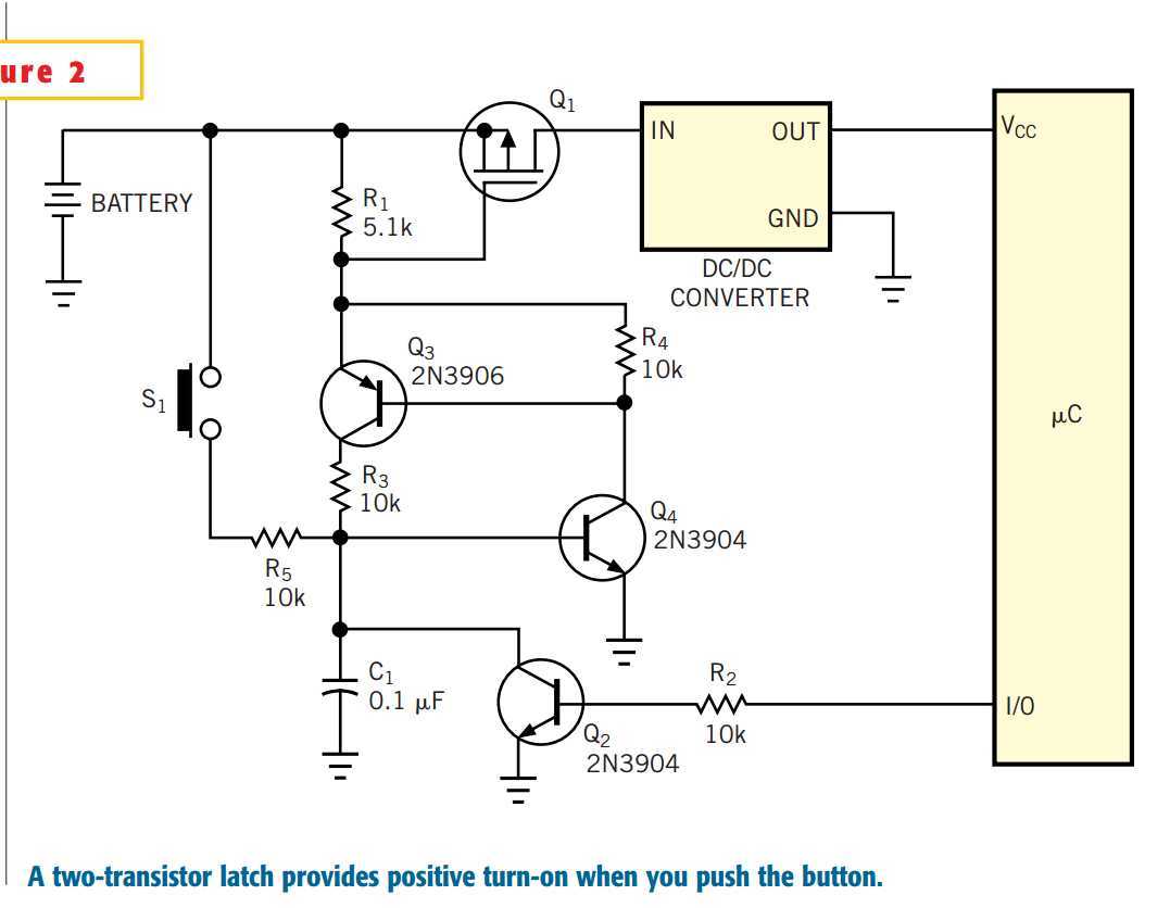
The circuit includes a simple two-transistor latch, which the On button switches to the on state. As in Figure 1, the p-channel MOSFET, Q1, serves as a power switch. When you push the On button, S1, it causes saturation of the npn transistor, Q4, via the base-current-limiting resistor, R5. The collector current of Q4 flows through R1 and the base-emitter junction of pnp transistor Q3, thereby saturating Q3. Q3 redirects some current into the base-emitter junction of Q4 and finishes the latching process. At this point, both Q3 and Q4 are saturated, and the voltage on the gate of Q1 is a function of the voltage drop across the base-emitter junction of Q3 and the saturation voltage of Q4. This voltage is approximately 0.9V. The µC need not confirm the on state of the latch. When the µC powers up and finishes its housekeeping start-up code, it programs the I/O pin to logic zero.
Later, when the µC decides to power itself off, it programs the I/O pin to logic one and stops. Q2 turns off Q4, resetting the latch to its initial off state. R4 lowers the equivalent input impedance of Q3. This function improves EMI and ESD noise immunity and prevents the circuit from turning itself on in the presence of strong electromagnetic fields. Capacitor C1 in combination with R5 protects Q4 and Q2 from direct ESD into the pushbutton. Some portable devices use undervoltage-lockout circuitry. This circuitry usually uses a voltage comparator with a built-in voltage reference. If the battery voltage drops below the threshold, the output of the comparator (usually an open-drain type) switches low. If your portable system uses this type of circuitry, you can connect the open-drain output of the comparator in parallel with Q2, thus preventing the latch from turning on if the battery voltage is too low.


Transistor latch improves on/off circuitry
标签:des blog http io ar os sp for strong
原文地址:http://www.cnblogs.com/shangdawei/p/4128478.html