标签:des style blog http tar ext
Mobile devices, such as but not limited to personal data appliances, cellular phones, radios, pagers, lap top computers, and the like are required to operate for relatively long periods before being recharged. These mobile devices usually include one or more processors as well as multiple memory modules and other peripheral devices.
In order to reduce the power consumption of mobile devices various power consumption control techniques were suggested. A first technique includes reducing the clock frequency of the mobile device. A second technique is known as dynamic voltage scaling (DVS) or alternatively is known as dynamic voltage and frequency scaling (DVFS) and includes altering the voltage that is supplied to a processor as well as altering the frequency of a clock signal that is provided to the processor in response to the computational load demands (also referred to as throughput) of the processor. Higher voltage levels are associated with higher operating frequencies and higher computational load but are also associated with higher energy consumption.
DVS can be implemented by software. A disadvantage of software based application results from timing issues and the computational load that an execution of such software imposes on a processor.
DVS can also be implemented by hardware. A disadvantage of hardware-based solution resides on their inflexibility and complexity.
Various DVS systems and method are provided at U.S. Pat. No. 6,584,571 of Fung, titled "system and method of computer operating mode clock control for power consumption reduction", U.S. Pat. No. 6,079,025 of Fung titled "system and method of computer operating mode control for power consumption reduction", U.S. patent application 20020042887 of Chauvel et al., titled "Dynamic hardware configuration for energy management systems using task attributes", all being incorporated herein by reference.
There is a need to provide a trade off between software and hardware based DVS apparatuses.
The invention provides a method and an apparatus for controlling voltage level and clock signal frequency supplied to a system. The apparatus includes a hardware module, adapted to receive at least one activity related signal representative of an activity of at least one component of the system and to determine a voltage level and a clock signal frequency to be provided to the system, and a software module, adapted to configure a voltage source and a clock signal source in response to the determination.
The following description related to a system that includes a single frequency region. It is noted that this can be applied to a system that includes multiple frequency regions. Typically, multiple frequency regions require separate control for each frequency region.
FIG. 1 is a schematic illustration of a system?100?that includes multiple components such as processor?110, memory bank?120, I/O modules?130, interrupt request controller?140, clock signal source?220, voltage source?210, synchronization control unit?230. System?100?also includes a hardware module?200. Conveniently, processor?110?executes a software module?300?that with the hardware module?200?forms apparatus?232.
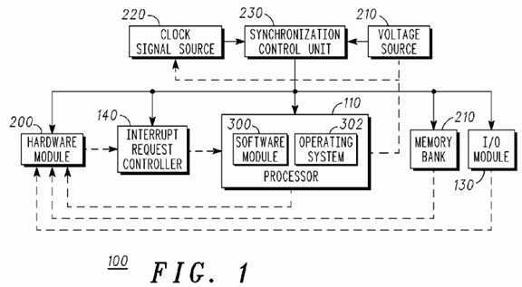
It is noted that system?100?can have various configurations and that the components illustrated in FIG. 1 represent only a single exemplary configuration of system?100. Typically system?100?is includes within a mobile device such as a cellular phone.
The hardware module?200?is adapted to receive one or more activity related signals representative of an activity of at least one component of the system?100?and in response determine whether to alter the voltage/frequency provided to the components of system?100. Such signals may include, for example, memory access signals (read/write), cache hit/miss signals, bus related signals, processor IDLE signal, various processor instructions, interrupt requests, I/O access, and the like.
Apparatus?232?is capable of determining the supply voltage and clock signal frequency supplied to system?100?(said characteristic pair is referred to as voltage/frequency) under various timing constraints that include, for example: the decision period of apparatus?232, voltage supply and clock signal supply stabilization period, and system‘s?100?and especially processor‘s?110?load change rate.
When the load of system?100?decreases a significant decrement of the voltage/frequency can amount in large power consumption reduction. Nevertheless, the reduction of voltage/frequency shall take into account the next (lower) voltage/frequency to supply to system?100.
When the load of system?100?increases, the voltage/frequency must be increased relatively fast in order to prevent performance penalties that are especially critical when the system?100?executes a real time program such as a video processing program.
In both cases the apparatus?232?must track the load of system?100?in a relatively fast manner but without introducing too many voltage/frequency changes.
The apparatus?232?can be adapted to apply a first policy when deciding to increase the frequency/voltage supplied to system?100?and a second policy, that conveniently differs from the first policy, when deciding to decrease the voltage/frequency supplied to system?100. It is noted that apparatus?232?can apply various policies, even the same or substantially the same policies when deciding to increase or decrease the supplied voltage/frequency.
Conveniently, applying different voltage/frequency increment and decrement policies are implemented, for example, by setting different average load thresholds (Nup and Ndown, Lp and Ldown) to various load related events. Those of skill in the art will appreciate that using the same (or substantially the same) voltage/frequency increment and decrement policies can include using the same average load thresholds, but this is not necessarily so.
FIG. 2 illustrates apparatus?232, according to an embodiment of the invention.
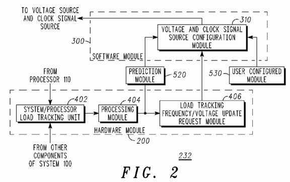
The various tasks associated with controlling and providing voltage and clock signals to system?100?were divided between the hardware module200?and the software module?300?of apparatus?232. The hardware module?200?receives one or usually multiple activity related signals, applies a load tracking algorithm such as but not limited to the exponential moving average (EMA) algorithm and determine when to alter the voltage/frequency supplied to system?100.
The software module?300?configures the voltage source?210?and the clock signal source?220.
Optionally, the apparatus?232?includes a prediction module?520?that predicts how to alter the voltage/frequency in response to previous exponential moving average load estimates. The hardware module?200?includes programmable components thus allowing alterations of the decision process.
The control of the voltage source?210?and clock signal source?220?is relatively simple and does not load the processor?110. Furthermore, its simplicity allows components having limited processing capabilities, such as DMA modules and simple controllers, to execute the voltage and clock signal source configuration module?310. In addition, various existing processors have the capability of setting voltage and clock signal frequency, thus utilizing this capability further increases the efficiency of apparatus?232?and system?100?as a whole.
The apparatus?232?samples the activity related signals by the clock signal CLK supplied to the system or by a clock signal having a lower frequency, such as CLK_3?that is a derivative of CLK.
Said sampling provides a more accurate load level tracking than a system that uses a real time clock that is not influenced by the changes of clock signals provided to the monitored system.
System?100?receives a supply voltage V(t) as well as a clock signal CLK of a certain frequency F(t) from a synchronization control unit?230?that synchronizes the levels of V(t) and F(t) such as to prevent, for example, a case in which the supplied voltage V(t) does not allow the system?100?to operate at a the frequency F(t) of the clock signal. The synchronization control unit?230?is connected to a clock signal source?220?for receiving the clock signal and is also connected to a voltage source?210?for receiving the supply voltage. Conveniently, the clock signal source?220?includes two phase locked loops, whereas while one is supplying a current clock signal of a current frequency the other can be tuned to supply the next clock signal having a next frequency. The voltage source can also include two voltage sources but this is not necessarily so.
Apparatus?232?includes a hardware module?200?that includes a system/processor load tracking unit?402, a processing module?404?and a load tracking frequency/voltage update request module?406. The software module?300?includes a voltage and clock signal source configuration module310. FIG. 2 also illustrates two optional modules such as prediction module?520?and user configures module?530, each can be a hardware module, a software module or a combination of both hardware and software.
The voltage and clock signal source configuration module?310?is capable of configuring the clock signal source?220?as well as the voltage source210?by various prior art methods, such as writing control values to registers accessed by these sources.
The voltage and clock signal source configuration module?310?is capable of receiving a requests to alter the voltage/frequency from load tracking frequency/voltage update request module?406?and to convert the request to a format that can be understood by and accessible to the clock signal source?220?as well as the voltage source?210.
Conveniently, the voltage and clock signal source configuration module?310?receives also a request to alter the voltage/frequency from a prediction module?520. According to another embodiment of the invention the voltage and clock signal source configuration module?310?is also adapted to receive requests from a user-configured module?530.
When requests can be provided to the voltage and clock signal source configuration module?310?from more that a single module it may apply various decision processes to decide how to alter the voltage/frequency. Each request can be assigned with a certain priority and/or weight and any combination of at least one of the requests can be applied. For example, a request of the prediction module?520?can override a request of the load tracking frequency/voltage update request module?406, and a request from the user-configured module?530?can override both.
System/processor load tracking unit?402?received multiple activity related signal and is capable of assigning a predefined weight to each signal. Conveniently, the system/processor load tracking unit?402?tracks the activity of the processor?100?by monitoring at least one signal such as an IDLE signal and also is also capable of tracking the activity of other components of system.
The a system/processor load tracking module?402?provides an indication of the activities of various components to a processing module?404?that outputs a load indication and an exponential moving average load estimate to the load tracking frequency/voltage update request module?406?and also provides the exponential moving average load estimate to the prediction module?520.
FIG. 3 is a schematic diagram of various modules?402-406?of the apparatus?232, according to an embodiment of the invention.
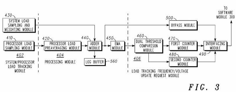
System/processor load tracking module?402?includes modules?410?and?430. Processor load sampling module?410?samples the IDLE or NON-IDLE (BUSY) signal of processor?110. The IDLE or NON-IDLE (BUSY) signal is sampled by CLK and creates IDLE′ sampled signal. Thes IDLE′ sampled signal is provided to a processor load pre-averaging module?420?that belongs to processing module?404. The processor load pre-averaging module420?calculates a ratio R between the amounts of clock signals (CLK) during a certain averaging period and between the amount of sampled signal IDLE′ provided by processor load sampling module?410?during that certain averaging period. The length of the averaging period is programmable. Conveniently, either module?410?or module?420?can multiple either IDLE′ or R by a programmable weight W_IDLE. Conveniently, the averaging periods do not overlap, but this is not necessarily so.
Conveniently, processor load pre-averaging module?420?also divides CLK to generate a slower clock signal CLK_3?that is provided to various modules such as modules?430?and?440-490.
System load sampling and weighting module?430?receives multiple activity related signals from other components of system?100, although it can also receive one or more signals (other than IDLE) from processor?110. The system load sampling and weighting module?430?samples the received signals by CLK_3?and multiplies each sampled activity related signal by a corresponding programmable weight to provide multiple weighted system activity related signals SL_1-SL_K.
R is also provided to a log buffer?560, and conveniently said log buffer?560?can also receive at least one of the load indication system load indication signals.
Processing module?404?includes modules?420,?440?and?450. Adder module?440?adds R to the multiple weighted system activity related signals SL_1-SL_K to provide a load indication LL(t).
The load indication LL(t) is provided to a bypass module?500?as well to a exponential moving average (EMA) module?450.
The EMA module?450?applies an exponential moving average module algorithm that is responsive to at least one programmable parameter α. Basically, EMA performs the following equation: EMA(t)=α*LL(t)+(1?α)*EMA(t?Δt), whereas EMA(t) is an exponential moving average load estimate, α=1/(W+1), W is a positive integer representative of an amount of samples that are taken into account within a programmable window and EMA(t?Δt) is a result of the previous iteration of an EMA calculation. Typically, Δt is responsive to CLK_3?and to an amount of clock cycles required for the calculation of EMA(t).
The inventors used an eight bit α, but this is not necessarily so. When α is increased the current value of LL(t) is more dominant thus rapid changes of LL(t) can be tracked. When α is decreased previous samples are more relevant and a more stable tracking process is achieved.
Load tracking frequency/voltage update request module?406?includes modules?460-480.
Load tracking frequency/voltage update request module?406?is adapted to apply different voltage/frequency increment and decrement policies. These different policies are applied by setting different thresholds like Lup and Ldown as well as using two different counters for counting consecutive EMA_higher_than_Lup signals and EMA_lower_than_Ldown signals. According to another embodiment of the invention the load tracking frequency/voltage update request can apply the same (or substantially the same) policies, for example by using a single threshold instead of using a lower threshold and an upper threshold, but this is not necessarily so.
Load tracking frequency/voltage update request module?406?receives exponential moving average load estimate EMA(t) and compares it in parallel to a upper average load threshold Lup and to a lower average load threshold Ldown. Both load thresholds are programmable. Higher Lup values lead to a slower voltage/frequency update process while lower Ldown values lead to an unstable voltage/frequency update process.
Each time EMA(t) exceeds Lup the dual threshold comparison module?460?generates a EMA_higher_than_Lup signal. The EMA_higher_than_Lup signal is sent to a first counter module?470?that counts the amount of consecutive EMA_higher_than_Lup signals. The first counter module?470generates a request to increase the voltage/frequency (Req_up(t)) if more than a programmable amount (N_up) of consequent EMA_higher_than_Lup signals were received.
Each time EMA(t) is below Ldown the dual threshold comparison module?460?generates a EMA_lower_than_Ldown signal. The EMA_lower_than_Ldown signal is sent to a second counter module?480?that counts the amount of consecutive EMA_lower_than_Ldown signals. The second counter module?480?generates a request to decrease the voltage/frequency (Req_down(t)) if more than a programmable amount (N_down) of consequent EMA_lower_than_Ldown signals were received.
Req_up(t) and Req_down(t) signals are provided to interfacing logic?490?that sets various status bits, accessible by software module?300, to reflect a received request to alter voltage/frequency. Interfacing logic can also send a request to interrupt request controller?140?(or directly to processor110) to initiate an interrupt request that enables processor?110?to execute voltage and clock signal source configuration module?310. The voltage and clock signal source configuration module?310?converts requests to increase or decrease voltage/frequency to commands that control the clock signal source?220?and the voltage source?210?accordingly.
The bypass module?500?receives LL(t) and compares it to a predefined load threshold. If said load threshold is exceeded the bypass module?500can send a request to increase the voltage/frequency to interfacing logic?490, regardless of the output of modules?450-480. The bypass module?500allows the apparatus?232?to respond quickly to sudden system overload situations.
The prediction module?520?can predict power consumption based upon previously stored load indications, for example the load indications stored at the log buffer?560.
According to other embodiments of the invention the prediction module?520?can response to instructions being executed by processor?100. For example, it may predict the load when processor?110?executes loops, by monitoring various commands, flow changes an/or loop commands fetched by processor?110. The prediction module?520?can include software components, hardware components or a combination of both.
According to an embodiment of the invention the programmable values provided to the apparatus?232?can be responsive to previously provided values and even to the tasks that are executes by system?100?and especially processor?110. For example, when system?100?mainly processes video the system?100?and especially processor?110?can load a first set of programmable values to the apparatus?232, while when executing other tasks, another set of programmable values can be loaded. The programmable values can be also programmed in response to previous voltage/frequency alterations. For example very frequent voltage/frequency alterations can indicate that a slower tracking process is required and vice verse. The programmable values can also be responsive to other parameters such as operating conditions (such as temperature, battery level) of system?100?and the like.
FIG. 4 is a flow chart of a method?600?for controlling voltage level and clock signal frequency supplied to a system.
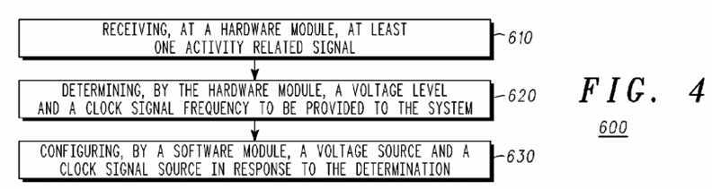
Method?600?starts by stage?610?of receiving, at a hardware module, at least one activity related signal. Conveniently, stage?610?includes assigning a weight to each activity related signal.
Referring to the example illustrated by FIG. 1-FIG.?3, the processor load sampling module?410?and the system load sampling and weighting module430?receive multiple signals representative of the activities of various components of system?100?including processor?110.
Stage?610?is followed by stage?620?of determining, by the hardware module, a voltage level and a clock signal frequency to be provided to the system.
Conveniently, stage?620?includes calculating an exponential moving average load estimate. Preferably, the exponential moving average load estimate is compared to an upper average load threshold and to a lower average load threshold. Referring to the example illustrated by FIG. 1-FIG.3, said determination is responsive to a calculation process applied by modules?420-480. According to another embodiment of the invention the method can include applying the same (or substantially the same) voltage/frequency policies, for example by using a single threshold instead of using an lower average threshold and an upper average threshold, but this is not necessarily so.
Conveniently, stage?620?further includes comparing a load indication to a load threshold and generating a request to increase the voltage level and clock signal frequency if the load indication exceeds the load threshold. Referring to the example set forth in FIG. 1-FIG.?3, this stage can be implemented by bypass module?500.
According to an embodiment of the invention stage?620?is followed by a stage of storing load indications.
According to yet another embodiment of the invention stage?620?includes estimating future load in response to the stored load indications.
Conveniently, the hardware module applies a first policy for increasing the voltage level and clock signal frequency and a second policy for decreasing the voltage level and clock signal frequency.
Stage?620?is followed by stage?630?of configuring, by a software module, a voltage source and a clock signal source in response to the determination. According to a further embodiment of the invention method?600?includes providing the clock signal to a first portion of the hardware module and providing another clock signal of a lower frequency to a second portion of the hardware module.
Conveniently, method?600?includes programming at least one programmable parameter of the hardware module.
SRC=http://www.freepatentsonline.com/7975155.html
PatentTips - Controlling voltage and frequency,布布扣,bubuko.com
PatentTips - Controlling voltage and frequency
标签:des style blog http tar ext
原文地址:http://www.cnblogs.com/coryxie/p/3793335.html