标签:des style blog http color strong
This invention relates in general to an integrated circuit and more specifically to well biasing circuitry for transistors of an integrated circuit.
Integrated circuits utilize transistors, such as e.g. CMOS transistors, for implementing logic circuitry of the integrated circuit. In one example, logic circuitry is implemented in rows of cells of an integrated circuit. These rows may contain N well areas and P well areas that are utilized to implement the transistors of the logic circuitry.
In some embodiments, during the normal operation of the integrated circuit, the N well area is biased with a supply voltage of VDD and the P well area is biased with a supply ground voltage VSS. For some transistor types, such as CMOS, the sub threshold leakage current of the transistors may be unacceptably large, such that the integrated circuit draws large amounts of current during standby. In order to reduce power during standby, the N well areas maybe biased with a voltage that is higher than the supply voltage VDD and the P well areas may be biased with a voltage that is lower than the supply voltage VSS. However, circuitry for selectively biasing the well areas of an integrated circuit may occupy an unacceptable amount of space of the integrated circuit and/or may generate a large amount of inrush current during a change in well bias voltages.
What is needed is improved circuitry for selectively biasing the well areas of an integrated circuit.
The following sets forth a detailed description of a mode for carrying out the invention. The description is intended to be illustrative of the invention and should not be taken to be limiting.
FIG. 1 is a partial top view of an integrated circuit according to the present invention. Integrated circuit?101?includes logic circuitry implemented in standard cells (e.g.?111) in a sea of gates?102?of integrated circuit?101. Sea of gates?102?includes a plurality of rows of cells with row of cells?103,105, and?107?being shown in FIG. 1. Row of cells?103?includes standard cells?109,?111,?113,?115, and?117. Row of cells?105?includes standard cells119,?121,?123,?125,?127, and?129. Row of cells?107?includes standard cells?133,?132, and?131. Each standard cell includes a plurality of transistors to implement a logic function of the integrated circuit. In one embodiment, these transistors are CMOS transistors. As will be discussed further, sea of gates?102?includes switching cells (e.g.?159) that allow the P well areas and the N well areas of the sea of gates to each be selectively biased at different voltages from the supply voltages.
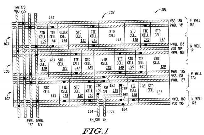
Each row of cells includes an N well area and a P well areas for implementing the transistors of the logic circuitry in the cells of that row. In one embodiment, the N well areas and the P well areas are doped regions of the semiconductor substrate of integrated circuit?101. For example, row of cells?103?includes P well area?169?which runs along the top portion of row of cells?103, relative to the view shown in FIG. 1, and a portion of N well area?171?which runs along the bottom of row of cells?103, relative to the view shown in FIG. 1. A portion of N well area?171?serves as the N well area for row of cells?105.
Each row of cells includes multiple tie cells (e.g.?141) for coupling a well area to a well bias line (e.g.?181?and?183) located in a metal layer above the substrate. For example, row of cells?103?includes tie cells?141,?143, and?145. Each of tie cells?141,?143, and?145?include a via-contact structure (e.g.?161?for tie cell?141) for coupling P well bias line?181?to P well area?169?and a via-contact structure (e.g.?163?for tie cell?141) for coupling N well bias line?183?to N well area?171. Via-contact structure?161?includes both a via and a well bias contact for coupling bias line?181, which in one embodiment is located in the second metal layer, to P well area?169?of the substrate. Row of cells?105?includes tie cells?147,?149, and?151?having via-contact structures for coupling N well bias line?186?to N well area?171?and for coupling P well bias line?185?to P well area?173. Row of cells?107includes tie cells?153,?155, and?158?having via-contact structures for coupling P well bias line?187?to P well area?173?and coupling N well bias line189?to N well area?175. P well areas?169?and?173?are biased by the voltage of the P well bias lines?181,?185, and?187. N well areas?171?and?175are biased by the voltage of N well bias lines?183,?186, and?189.
As shown in the embodiment of FIG. 1, the tie cells in each row of cells are non uniformly spaced from each other. This non uniformity of spacing of the tie cells is due to their placement in areas of the rows of cells that are not occupied by standard cells. The ability to place the tie cells in a non uniform placement aids in the flexibility of the layout of sea of gates?102. In one embodiment, the tie cells are placed in a row such that they are located no further than a certain distance of each other. In one embodiment, the tie cells are located no further than 186 microns from each other in a cell.
The P well bias lines?181,?185, and?187?are coupled together by vertical P well bias line?177, which is located in a higher metal layer (e.g. metal layer?3). N well bias lines?183,?186, and?189?are coupled together by vertical N well bias line?179, also located in metal layer?3?in one embodiment. Vertical bias lines?177?and?179?are coupled to a charge pump circuit (e.g.?307?of FIG. 3) and can be selectively supplied with voltages VPW and VNW, respectively, that are lower than VSS and higher than VDD, respectively, so as to selectively bias the P well areas and N Well areas at VPW and VNW, respectively. In one embodiment VDD is 1.5 V, VSS is 0V, VNW is 2.1 volts and VPW ?1.0V. However in other embodiments, VNW maybe less than VDD and/or VPW maybe greater than VSS.
Horizontal VDD supply voltage lines?184?and?195?are located in the first metal layer and are coupled together by an upper layer vertical VDD line176. Horizontal VSS supply voltage lines?180?and?198?are located in the first metal layer and are coupled together by an upper layer vertical VSS line?178. These supply voltage lines supply the cells with supply voltages VDD and VSS.
Sea of gates?102?includes switching cells (e.g.?159) for coupling the P well bias lines (e.g.?187) to the VSS voltage lines (e.g.?198) and for coupling the N well bias lines (e.g.?189) to the VDD voltage lines (e.g.?195) in response to a state of an enable signal on enable line?174. These switching cells enable the well areas to be selectively biased, based upon the enable signal, to the supply voltages VDD or VSS or to voltages VNW and VPW.
FIG. 2 is a circuit diagram of switching cell?159. Switching cell?159?includes a PMOS coupling transistor?203, which serves as a switch for coupling N well bias line?189?to VDD line?195?through via-contact structures?193?and?194. Via-contact structure?193?is also coupled to P well area?173?(see FIG. 1). Switching cell?159?also includes an NMOS coupling transistor?205?for coupling P well bias line?187?to VSS line?198?through via-contact structures?190?and?191. Via-contact structure?190?is also coupled to N well area?175?(see FIG. 1).
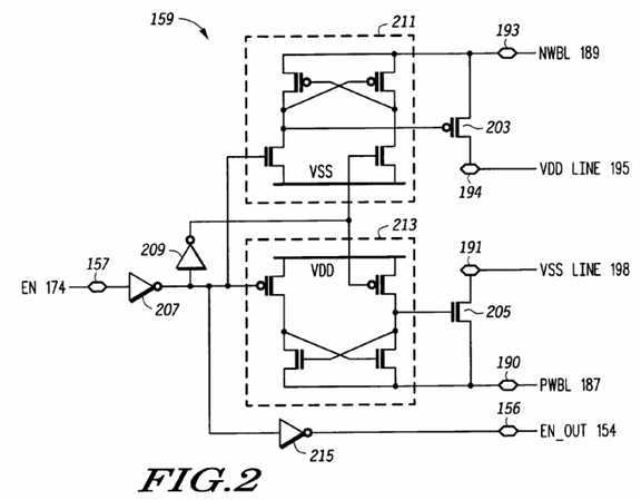
Switching cell?159?receives an enable signal from enable line?174?through via-contact structure?157. The enable signal controls whether or not coupling transistors?203?and?205?are conductive to couple line?189?to line?195?and line?187?to line?198, respectively, to bias N well areas?175?and171?to VDD and to bias P well areas?173?and?169?to VSS, respectively. When the signal on enable line?174?is high (e.g. VDD), transistors?203?and205?are non conductive. When the signal on enable line?174?is low (e.g. VSS), transistors?203?and?205?are conductive.
Switching cell?159?also includes two level shifters?211?and?213?for supplying a voltage to the gates of transistors?203?and?205, respectively, to maintain the non conductivity of transistors?203?and?205?when the enable signal is in a state (VDD in the embodiment shown) for non conductivity. When the signal on line?174?is at a high state (e.g. VDD) where the transistors?203?and?205?are to be non conductive, the output of inverter?209?is also at a high state, which pulls the voltage of the gate of transistor?203?to the voltage level of N well bias line?189?(which is at VNW at that time). Accordingly, when line?189?is at VNW, the gate of transistor?203?is also at VNW, thereby maintaining the non conductivity of transistor?203. Likewise when enable signal on line?174?is at a high voltage state, the gate of transistor?205?is pulled to the voltage of line?187, which at that time is at VPW, and which is at lower voltage (e.g. ?1.0V) than VSS (e.g. 0V).
Providing a switching cell with two coupling transistors responsive to a control line may enable a switching cell to selectively couple the N well bias line to the VDD line and selectively couple the P well bias line to the VSS line with only one control signal line (e.g. on line?174). Accordingly, the number of control signals needed to be routed in the metal layers for selective well biasing may be reduced, thereby saving area in the sea of gates.
Switching cell?159?also includes a control output (e.g. coupled to via-contact structure?156) that is coupled to the output enable line (En_Out)?154for providing the enable signal to a next switching cell (e.g.?312?in FIG. 3) of sea of gates?102?whose control input (e.g. the line connected to via-contact structure?157?for switching cell?159) is coupled to line?154. In the embodiment of FIG. 2, invertors?207?and?215?located between via-contact structure?157?and via-contact structure?156?provide a delay in the enable signal before being provided to the next sequentially coupled switching cell (e.g.?312) located in sea of gates?102. One advantage that may occur from providing a delay in the enable signal is that it may allow each switching cell to bias the N well areas and P well areas with the VDD supply voltage and VSS supply voltage, respectively, at staggered times. Such staggering may limit the in rush current due to the change in voltage of the N well areas and P well areas in that all of the switching cells of a sea of gates do not couple the N well areas to VDD and P well areas to VSS at the same time.
FIG. 3 is a block diagram of integrated circuit?101. In one embodiment, integrated circuit?101?is an application processor. Integrated circuit?101includes a memory?303, which in one embodiment, is located in an area of integrated circuit?101?that does not include circuitry for selectively biasing its N well areas and P well areas.
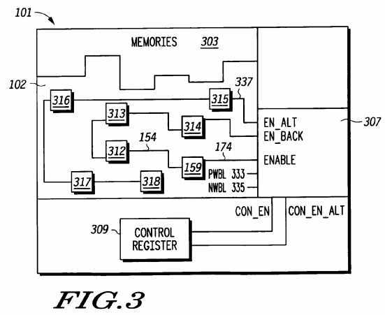
In the embodiment of FIG. 3, sea of gates?102?includes two sets of sequentially coupled switching cells. The first set includes switching cells?159,312,?313?and?314, and the second set includes switching cells?315,?316,?317, and?318. Each of these switching cells is similar to switching cell?159as shown in FIG. 2. Each set is sequentially coupled in that the control output (e.g. the line connected to via-contact structure?156?for switching cell159) for a preceding switching cell in the sequence (e.g. switching cell?159) is coupled to the control input (e.g. the line connected to via-contact structure?157?in switching cell?159) of the next switching cell in the sequence. For example, switching cell?312?is the next switching cell in the sequence after switching cell?159. Accordingly, signal line?154?is coupled to the control input of switching cell?312.
Each switching cell in sea of gates?102?is located at a different area of sea of gates?102. Each switching cell can effectively couple the voltage supply lines carrying VDD and VSS to the N well areas and P well areas, respectively, for a given area. Accordingly, in one embodiment, the switching cells are spaced such that all of the sea of gates?102?is covered by an effective area of a switching cell. In the embodiment shown, the switching cells are placed in a non uniform pattern. The ability to place the switching cells in a non uniform pattern may allow for greater flexibility in the design of integrated circuit?101. In some embodiments, the effective area of a switching cell is dependent upon the process technology and the size of the coupling transistors of the switching cell.
Integrated circuit?101?includes a control register?309?whose contents control whether the N well and P well areas of sea of gates?102?are to be biased with the supply voltages VDD and VSS or the well bias voltages VNW and VPW. In the embodiment shown, control register?309?provides a first output signal CON_EN to control the conductivity of the PMOS and NMOS coupling transistors (e.g.?203?and?205?of switching cell?159) of the first set of switching cells (159,?312,?313, and?314) and provides a second output signal CON_EN_ALT for controlling the conductivity of the PMOS and NMOS coupling transistors of the second set of switching cells (315,?316,?317, and?318). In one embodiment, control register?309?is a control register of the clock control module (not shown) of integrated circuit?101. In some embodiments, the contents of register?309?may be set by a processor core (not shown) executing code, either internally or externally stored with respect to integrated circuit?101, or by firmware. In other embodiments, control register?309?may only provide one signal for controlling the bias voltages of the well areas of sea of gates?102.
Integrated circuit?101?includes a charge pump circuit?307?that provides an enable signal (ENABLE) to line?174?to control the conductivity of the PMOS and NMOS coupling transistors of the first set of switching cells (159,?312,?313, and?314) in response to the CON_EN signal received from control register?309. Charge pump circuit?307?also provides a second enable signal EN_ALT to enable line?337?for controlling the conductivity of the PMOS and NMOS coupling transistors of the second set of switching cells (315,?316,?317, and?318) in response to the CON_EN_ALT signal.
Charge pump circuit?307?includes an input for receiving the enable signal (EN_BACK) from the control output (e.g. the line connected to via-contact structure?156) of switching cell?314. With some embodiments, this signal can be used to indicate whether a change in state of the enable signal ENABLE has propagated through all of the switching cells of the first set of switching cells. In other embodiments, charge pump circuit?307?may also receive a signal from the control output of switching cell?318.
Charge pump circuit?307?also includes outputs coupled to P well bias line?333?and N well bias line?335?for selectively providing on those lines the VPW voltage and the VNW voltage, respectively, to bias the P well areas of sea of gates?102?and to bias the N well areas of sea of gates?102, respectively. P well bias line?333?is coupled to P well bias line?177?and N well bias line?335?is coupled to N well bias line?179?(see FIG. 1).
FIG. 4 is a block diagram of charge pump circuit?307. Charge pump circuit?307?includes a controller?413?that receives the CON_EN and CON_EN_ALT signals from control register?309?and receives the EN_BACK signal from switching cell?314. Controller?413?also provides the ENABLE signal and the EN_ALT signal.
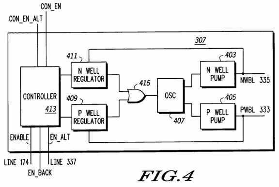
Charge pump circuit?307?includes an N well charge pump?403, that when activated, provides at its output the VNW voltage on line?335. Charge pump circuit?307?also includes a P well charge pump?405, that when activated, provides at its output the VPW voltage on line?333. When charge pumps?403?and?405?are not activated, their outputs are tri-stated.
Charge pump circuit?307?includes an oscillator?407, that when turned on, activates charge pumps?403?and?405. Oscillator?407?is turned on through OR gate?415?by either N well regulator?411?or P well regulator?409. Regulator?411, when turned on by controller?413, turns on oscillator?407?in response to the voltage of the output of charge pump?403?falling below a predetermined voltage level. Regulator?409, when turned on by controller413, turns on oscillator?407?in response to the voltage of the output of charge pump?405?rising above a predetermined voltage level. With other embodiments, regulator circuits having other configurations may be used.
When integrated circuit?101?is operating in a normal operating mode with the P well areas of sea of gates?102?biased to VSS and the N well areas of sea of gates?102?biased to VDD, the processor core (not shown) of integrated circuit?101, in one embodiment, initiates the placement of sea of gates102?in a standby mode where the N well areas are biased at VNW and the P well areas are biased at VPW. This initiation is accomplished by writing a value to control register?309?to place the CON_EN signal in a state to make non conductive the PMOS and NMOS coupling transistors of the first set of switching cells (159,?312,?313, and?314) and to place the CON_EN_ALT signal in a state to make non conductive the PMOS and NMOS coupling transistors of the second set of switching cells (315,?316,?317, and?318). In response to the CON_EN signal and the CON_EN_ALT signal changing states, Controller?413?places the ENABLE signal in a state to sequentially make the PMOS and NMOS coupling transistors of the first set of switching cells (159,?312,?313, and?314) non conductive and places the EN_ALT signal in a state to sequentially make the PMOS and NMOS coupling transistors of the second set of switching cells (315,?316,?317, and?318) non conductive. Making the PMOS and NMOS coupling transistors of the switching cells of sea of gates?102?non conductive decouples the P well bit lines of sea of gates?102?from VSS and decouples the N well bit lines of sea of gates?102?from VDD. In other embodiments, the states of the CON_EN signal and the CON_EN_ALT signals may be changed at different times during a transition from a normal operating mode to a standby operating mode.
When the EN_Back signal has changed states due the change in state in the ENABLE signal (and thus indicating that the coupling transistors of the first set of switching cells have been made non conductive), Controller?413?then turns on regulators?411?and?409?which turn on oscillator?407?to activate N well charge pump?403?and P well charge pump?405?to provide the voltage VNW on line?335?and VPW on line?333, respectively. Providing VNW on line?335?and VPW on line?333?with the coupling transistors of the switching cells being nonconductive biases the N well areas of sea of gates?102?at VNW and biases the P well areas of sea of gates?102?at VPW respectively.
To transition from a standby mode wherein the N well areas are biased at VNW and the P well areas are biased at VPW to a normal operating mode where the N well areas are biased at VDD and the P well areas are biased at VSS, control register?309?changes the state of the CON_EN signal. In response, controller?413?disables regulators?411?and?409?such that they turn off oscillator?407. With oscillator?407?off, the outputs of pumps?403?and405?(coupled to lines?335?and?333, respectively) become tri-stated. Controller?413?then changes the state of the ENABLE signal to a state to begin sequentially making the coupling transistors of the first set of switching cells conductive to couple the N well bias lines (e.g. 189) to the VDD voltage supply lines (e.g. 195) and P well bias lines (e.g. 187) to the VSS voltage supply lines (e.g. 198). In one embodiment, after a predetermined period of time, control register?309?changes the state of the CON_EN_ALT signal. In response, controller?413?changes the state of the EN_ALT signal to a state to begin sequentially making the coupling transistors of the second set of switching cells conductive to couple the N well bias lines to the VDD voltage supply lines and the P well bias lines to the VSS voltage supply lines.
Sequentially making conductive the coupling transistors of the switching cells may reduce the inrush current from coupling the bias well areas to the voltage supply lines. Providing two sets of independently controlled switching cells may enable the processor core (not shown) to have some control over the inrush current in that it can determine when the coupling transistors of the second set are made conductive. Thus, the time at which the coupling transistors of the second set are made conductive may be programmable or may be made in response to a measured parameter (e.g. measured current). In other embodiments, a sea of gates may include only one set of sequentially coupled switching cell or multiple sets of switching cells. Still in other embodiments, controller?413?may make the coupling of the coupling transistors of the second set conductive in response to a change in state of the EN_BACK signal due to a change in state of the ENABLE signal.
FIG. 5 is a flow diagram for one embodiment for the design of an integrated circuit according to the present invention. In one embodiment, the flow of FIG. 5 is implemented with computer aided design tools.
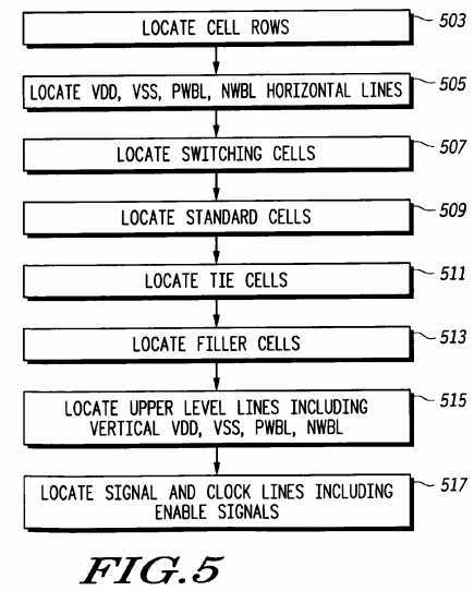
In?503, the locations are established for the rows of cells in a sea of gates on a substrate of an integrated circuit. In?505, the layout is set for the horizontal VDD lines, horizontal VSS lines, horizontal P well bias lines, and horizontal N well Bias lines in the first metal layer. In?507, the locations of the switching cells in the sea of gates is established. The switching cells are located such that all of the sea of gates is covered by an effective area of a switching cell.
In?509, the standard cells of the logic circuitry are located in the row of cells. In?511, tie cells are located within non designated spaces in the row of cells. In one embodiment, the tie cells are to be placed within a certain distance of each other. In?513, filler cells are located in the non designated spaces of the rows of cells. In?513, the locations of the upper level lines including the vertical VDD lines, the vertical VSS lines, the vertical P well bias lines, and the vertical N well bias lines are set. In?517, the signal and clock lines locations are set including the ENABLE, EN_ALT, and EN_BACK signals.
In other embodiments, an integrated circuit according to the present invention maybe designed by other processes.
With other embodiments, the well bias circuitry shown and described herein may be utilized to change the bias of the N well areas and P well areas for other operating modes of the integrated circuit. For example, the bias of the N well areas and P well areas of a sea of gates may be changed to adjust the threshold voltages of the transistors of a sea of gates during a normal operating mode. In other embodiments, the control inputs of each switching cell in an array are coupled together in parallel.
In one aspect of the invention, an integrated circuit includes a plurality of rows of cells. Each row of cells of the plurality includes a P well area and an N well area. The integrated circuit includes a plurality of P well bias contacts to bias the P well areas, a plurality of N well bias contacts to bias the N well areas, a first plurality of lines to carry a first voltage, a second plurality of lines to carry a second voltage, and a plurality of switching cells. Each switching cell is located in a row of cells of the plurality and is coupled to a line of the first plurality of lines, a line of the second plurality of lines, an N well bias contact of the plurality, and a P well bias contact of the plurality. Each of the plurality of switching cells includes a control input. In response to the control input being at a first state, the switching cell couples the line of the first plurality of lines to the N well bias contact of the plurality and couples the line of the second plurality of lines to the P well bias contact of the plurality.
In another aspect of the invention, an integrated circuit includes a row of cells including a doped well area, a well bias contact to bias the doped well area, a first line to carry a first voltage, and a switching cell located in the row of cells. The switching cell is coupled to the first line and the well bias contact. The switching cell includes a switch, a control input, and a level shifter. A first terminal of the switch is coupled to the first line, and a second terminal of the switch is coupled to the well bias contact. In response to the control input being at a first state, the level shifter provides a voltage equal to a voltage of the second terminal to a gate of the switch to make the switch non conductive.
In another aspect of the invention, an integrated circuit includes a plurality of rows of cells. Each row of the plurality of rows of cells includes a doped well area of a plurality of well doped areas. The integrated circuit includes a plurality of well bias contacts to bias the doped well areas of the plurality, a first plurality of lines to carry a first voltage, and a plurality of switching cells. Each switching cell of the plurality is located in a row of cells of the plurality of rows of cells. Each switching cell is coupled to a line of the first plurality of lines and a well bias contact of the plurality of well bias contacts. Each switching cell includes a control input. In response to the control input being at a first state, the switching cell couples the line of the first plurality of lines to the well bias contact of the plurality of well bias contacts. A first switching cell of the plurality of switching cells includes a control output coupled to a control input of a second switching cell of the plurality of switching cells. The control output of the first switching cell is responsive to the control input of the first switching cell.
In another aspect of the invention, an integrated circuit includes a row of cells including a P well area and an N well area, a P well bias contact to bias the P well area, an N well bias contact to bias the N well area, a first line to carry a first supply voltage, a second line to carry a second supply voltage, and a switching cell located in the row of cells. The switching cell includes a first switch coupled to the first line and the N well bias contact. The switching cell includes a second switch coupled to the second line and the P well bias contact. The switching cell includes a control input. In response to the control input being at a first state, the first switch is conductive to couple the first line to the N well bias contact to bias the N well area at the first supply voltage and the second switch is conductive to couple the second line to the P well bias contact to bias the P well area at the second supply voltage. In response to the control input being at a second state, the first and second switches are non conductive to enable the N well area to be biased at a voltage different from the first supply voltage and to enable the P well area to be biased at a voltage different from the second supply voltage.
SRC=http://www.freepatentsonline.com/7170116.html
PatentTips - Integrated circuit well bias circuitry,布布扣,bubuko.com
PatentTips - Integrated circuit well bias circuitry
标签:des style blog http color strong
原文地址:http://www.cnblogs.com/coryxie/p/3835295.html